More Photo Diode Amplifier – Investigating Miller Capacitance
In response to my posting of 31st December, my mate Nigel Machin left a comment that he thought that the miller capacitance of the voltage gain stage (Q2 in the CA3127 implementation, and Q11 in the discrete transistor version) would provide the dominant pole. The whole idea of this circuit was to have no pole dominant over that provided by the photo diode capacitance. The CA3127 transistors have hFE of 1 GHz, whereas my BC847s are a lot slower, and in simulation (but not in the hardware of the product) there was a little peak, indicating conjugation of closed loop poles.
I wanted to investigate this just a little further. Here are two moves I made in the LTSpice environment to understand this circuit a little better.
First, I wanted to open the loop. This circuit relies on a closed loop for DC conditions, so we need a loop that is closed at low frequencies and open in the frequency range of interest (where the diode capacitance and the the miller capacitance are introducing poles).
So here is the first move.
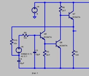
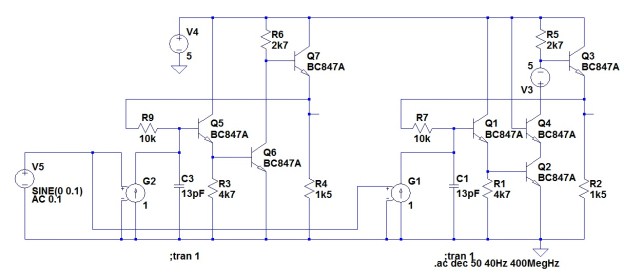
The voltage generator V5 will be where I will introduce the AC signal for the Bode plot. The minus end of this is where the low frequency feedback is introduced. The feedback will reduce the gain, but when you see the Bode plot later you will see that the low frequency fall off in gain is decades away from the frequencies of interest. R10 will represent the loading that is applied to the emitter of the emitter follower in the real circuit. The emitter of the emitter follower is where I have opened the loop for high frequency considerations. R9 represents the feedback resistor in the real circuit, in its role as part of the loop. C3 is the capacitance of the photo diode.
Now this circuit gives me a path around the feedback loop but with the loop open, starting from the signal fed to the feedback resistor (Left end of R9) and then through the forward path to the emitter of the emitter follower output stage.
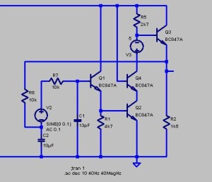
The second move is to do the same thing again, but to make a huge reduction in the Miller capacitance. I have done this by replacing the voltage gain stage (Q6 above) by a cascode.
I have chosen the 5 volt rail as a suitable point to tie the base of the top cascode transistor. This means that, allowing for some voltage swing, I need the collector of the top cascode transistor to be at a voltage that is somewhat higher then 5 volts. Fortunately, in the model world, we can pull stunts that would be tricky with real hardware, and I have raised the voltage of that collector with the fully floating voltage generator V3. The minus end of this will be at about 4.4 volts, so the plus end, the cascode transistor collector, will be at about 9.4. That will do nicely.
Now instead of having a voltage gain of about -100, Q2 will have a voltage gain round about -1.
This will reduce the impact of the Miller capacitance on the base of Q2 by a factor of 2/101. I built both of these circuits in a single model, which is just a simpleton’s way of providing for both Bode plots on the same axes.
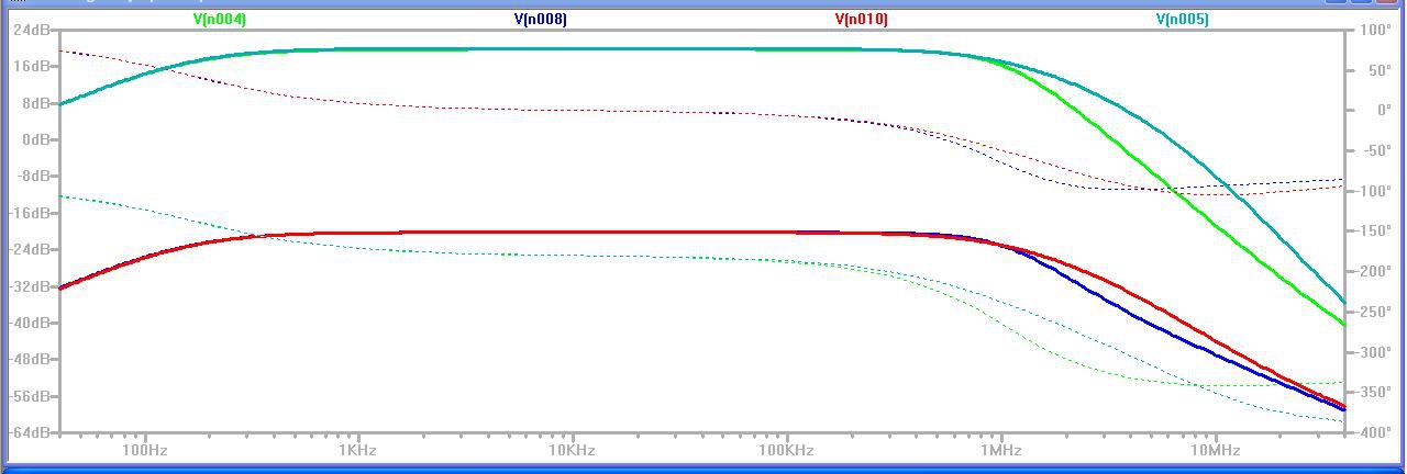
Here are the Bode plots
The colours are:
Dark Green – Open Loop gain of cascode Circuit (emitter of Q3)
Light Green – Open Loop gain of original circuit (emitter of Q7)
Red – Voltage at photo diode (C1) in cascode circuit
Blue – Voltage at photo diode (C3) in original circuit.
Notice that where the Blue line is lower than the Red line, this means that the Miller capacitance is lowering the impedance at the diode (and this effect is greater without the cascode), even though there is that input emitter follower in between.
The time constant in the open loop path that is presented by the feedback resistor and the photo diode capacitance is 130 ns, which corresponds to ω = 7.7E6, and f = 1.22 MHz. (this is ignoring the impedance presented by the base of the first stage, which we know has some capacitive component.)
It is interesting that the phase margin for both circuits is about the same – 20 degrees, although the Cascode has unity gain at a little over 6 mHz, and the original circuit has unity gain at a little over 3MHz.


