Foreword
This post has been delayed, not through any problem getting the content together, but by problems presenting the content on the BLOG page. My good friend Andrew Beal has been helping me with those problems. They are not all solved yet, but I am publishing this now (19-04-2015) as I am concerned that what is actually posted has fallen too far behind with thinking out material for this blog. As I attain more mastery over my formatting problems, I will come back and knock this post into better shape. And now, to the post…
Class C Part 1.
It used to be that much was made of the division of the bias arrangements for active devices into three classes. Class A, Class B and Class C. Some feature had to be found to easily distinguish these. The feature that was usually used was the proportion of a signal waveform for which the active device was conducting. This was expressed in degrees. Thus it was said that a Class A stage conducted for 360 degrees of the waveform, a Class B stage conducted for 180 degrees of the waveform, and a Class C stage conducted for less than 180 degrees of the waveform. In the case of vacuum tubes, there were many divisions between these. Thus we had push pull amplifiers classed as AB1, AB2 etc. It all depended on how one contrived to pass the amplifying task from one active device to the other at the zero crossing. These “intermediate classes” are explained in detail in The Radiotron Designers’ Handbook Chapter 13 Sections 1 and 7 (1).
It has been shown by Douglas Self (2) that when junction transistors are used as the active devices, there is no advantage in attempting to find an optimum with a compromize between the classes, and it is best if a linear amplifier is required, to commit to either Class A or Class B. An optimum design of a Class B stage has such a small output device quiescent current that it doesn’t warrant any subscripts after the B.
I have never designed a Class B MOSFET amplifier, but I have been reliably informed by one who has, that there is a particular trick. MOSFETs do not suddenly snap from their linear operation value of gm to zero as they pinch off, but go through a gradual transition. In an amplifier with a push pull complementary pair of Class B MOSFETs they are biased so that with zero signal, both output MOSFETs are sitting on their transition between linear operation and “off” so that each is exhibiting a gm value of half that for linear operation. At this point, they are both conducting (a little) and contributing half of the combined gm each.
As I see it, the number of degrees of the sine wave cycle is not really a definitive measure. All we can say is that active devices are set up to take half the signal each: one takes the positive half waveforms, and the other the negative half waveforms. Class B amplifiers have an efficiency advantage, partly because they exploit very particular properties of an audio signal.
An audio signal:
(a) Hovers about zero and deviates from this in both polarities in a more or less symmetrical pattern.
(b) Has a wide dynamic range. This means that an amplifier that has to meet some particular maximum power requirement will spend a lot of time delivering much lower output power.
Class C.
This is traditionally defined as an amplifier design style in which the active device is conducting for less than 180 degrees of the waveform cycle. This class evolved in a very particular application: the power amplifier for a radio transmitter. This application also has some very restrictive features the key one being that the bandwidth of the signal is small compared with the centre frequency.
This means that the amplification stage can be designed with an eye to maximum efficiency and very little (or none at all) effort to minimize distortion. The waveform distortion can then be reduced by a tuned circuit at the output. The tuned circuit that does this waveform restoration is called the “Tank Circuit”. I wonder how that term originated. (The expression “Tank Circuit” does not appear in my hard copy OED. It is to be found at http://www.merriam-webster.com/dictionary/tank%20circuit but without attribution.)
It seems that it is relatively easy to build a tuned circuit that has a high enough Q to make a practical approximation to a sine wave when being driven by a non-sinusoidal periodic waveform, and yet a low enough Q to accommodate the sidebands when amplitude modulation is applied. After all, the second harmonic of the carrier is usually a lot further away than the upper sideband.
There is even an opportunity to exploit the steeply falling spectrum of most audio material. This makes it possible to boost the high frequency end whilst making very little increase in the peak value of the composite waveform. This means that it would be possible to choose a Q for the tank circuit that is so high that the extremes of the sidebands are attenuated, but then compensate for this with pre-emphasis in the audio channel before the modulator. This would be a very minor step compared with the spectoral shaping, dynamic range reduction (compressing and limiting) and peak to RMS ratio reduction jiggery pokery that routinely goes on in AM transmitters.
It is always possible to add low pass filtering to further reduce the harmonics introduced in the Class C stage, and perhaps the “pi coupler” used for impedance matching, provides some low pass filtering at no extra cost.
Once freed of the requirement for linearity, and with a focus on high efficiency, we need an active device that acts like a switch. It is either a zero ohm conductor, or an open circuit, and it does not dally about wasting energy in some intermediate state. This sort of requirement is very familiar to us in these days of solid state devices and switched mode power supplies. It might have been obvious in the days of yore, but with thermionic devices, this was an ideal that must have seemed very remote. Designers had to make do with what they had.
There are two complementary ways we can add energy to the tuned tank circuit without interfering with its tuning or severely lowering its Q. One is to introduce a periodic waveform voltage in series with the L and C, and the other is to introduce a periodic current waveform to the parallel tuned circuit.
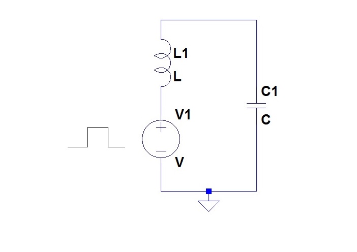
Tuned Circuit with Voltage Drive

Tuned Circuit with Current Drive
The scheme of driving the tuned circuit with a current is the scheme used in linear rf amplifiers in receivers, of course, where the high resistance of a pentode anode, collector or drain approximates the current source. The use of current drive is much more difficult in an environment where high efficiency is required. I have experimented (in simulation) with a circuit where a switched current is derived from an inductor. It came out as a circuit of a boost regulator, but with a tuned circuit instead of a reservoir capacitor on the output. Both switches have to be active switches (can’t use a diode for one of them as in a conventional boost stage), but the biggest problem is that the inductor that provides the current to the tank circuit, also detunes it. This could be corrected for, but only in a circuit where the duty cycle is fixed.
The one thing, we cannot do to provide energy to the Tank Circuit is to periodically connect it to a voltage source via a resistor. One would think that if the resistor value were low enough to transfer energy effectively into the tank circuit, then it would be low enough to lower the Q.
Yet, this is exactly what a traditional Class C output stage does.
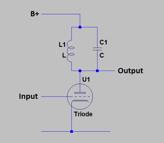
Triode in Class C
Sometimes a pentode is used, but the higher dynamic plate resistance is of no use here. When the valve is conducting, it is “hard on”. The high resistance available from the pentode when biased in the linear region is not available. One supposes that the lower Miller capacitance of the pentode might be a benefit. (And Possibly lower “On resistance” – see below.)
So the valve is used in a very unsuitable way, but possibly in the only way that was available given the characteristics of valves. When a valve is used as the active device, the characterizing feature of “conducting for less than 180 degrees of the waveform” arises. Here is a model circuit that I have used to investigate the effect of varying conduction angle.
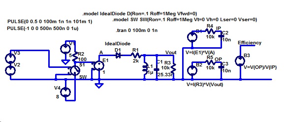
This is a bit much to take in as (unfortunately) my crude circuit drawing graphics capability makes for bad presentation of much data in the available width. I will quickly run through this model a section at a time.
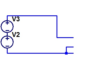
This very uninformative circuit segment will become clear when I explain it. V2 is a voltage generator that provides the 1 Megahertz signal as a triangle wave. V3 imposes a ramp. The combined effect is a triangle wave with a slowly increasing offset. To a following circuit that is sensitive only to whether the result is positive or negative, the result is a pulse train at 1 MHz that varies from zero to 50% duty cycle.
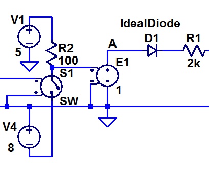 This part represents the supply and the valve. The voltage controlled switch is set up to vary with the control voltage in such a way that it reproduces the pulse train as described above. The 100 ohm resistor R2 and the two supplies V1 and V4 turn this into a pulse train that is at 5 volts during what we are representing as the “on” time, and minus 8 volts otherwise. The minus 8 volt supply is not part of the valve modelling, but is required to make the rest of my model work. It stops the ideal diode D1 from conducting during the “off” time. R1 represents the valve “on” resistance. You will observe that none of the voltages or resistances in my model have realistic values. I worked on this model until it worked. I have not spent further time rescaling it.
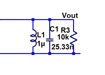 Here is the Tank Circuit and the load.
The final part is that which measures the efficiency.
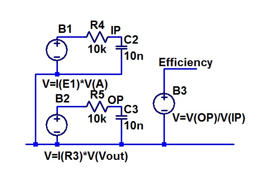
The arbitrary behavioural voltage source B1 has an output voltage that is the product of the valve current and voltage. It thus represents the instantaneous power being provided by the power supply of the transmitter. The resistor R4 and capacitor C2 give us a represtation of this averaged over several cycles.
Similarly B2 provides a voltage representing the product of the current and the voltage in the load. In other words instantaneous output power. R5 and C3 give us a represenation of this averaged over a few cycles.
The third arbitrary behavioural voltage source, has an output voltage that is the ratio of output power over power supply power, or in other words, efficiency.
here is the result.
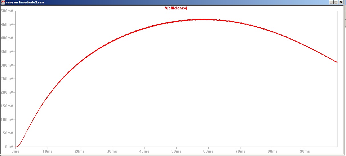
We can see that the maximum efficiency (of about 47 percent in this case) occurs when the duty cycle is about that obtained 0.6 of the way through the run. That is 0.6 of 180 degrees or 108 degrees. There you have it: for maximum efficiency for a valve in Class C, we can turn it on for about 108 degrees of the carrier waveform cycle.
This is an outcome that agrees remarkably well with actual historic practice, given the crudeness of my model, but I do not regard it as definitive. I would define Class C this way:
A Class C amplifier is one suited to a narrow band fixed frequency signal. The valve is driven so as to provide a switching type of waveform without regard to distortion, and then the signal is recovered from the harmonics by a high Q tuned circuit called the Tank Circuit.
This is the 21st Century, and we are well into the solid state era. How does that affect this style of amplifier?
When I was a youngster, I spoke to a bloke who had built a low power AM Broadcast transmitter. It was for use on an island, and I believe the figure of 100 watts was mentioned. The Class C valve was an 807.
I asked him about the common practice (which he had followed) of placing the modulator on the very output of the transmitter. This is an expensive practice, as it requires two high powered amplifiers – a Class C RF amplifier and a (usually Class B push pull) audio amplifier.
“You have to place the modulator on the output because with Class C there is too much distortion” he said.
I contend that when simply put like this, this statement is nonsense. Can I justify that?
Answers to these two questions in the next post.
Footnote 1. F. Langford-Smith (ed) – The Radiotron Designer’s Handbook Fourth Edition.
2. Douglas Self – Audio Power Amplifier Design Handbook Chapter 6.
Postscript.
there has been a little delay in posting this, and that has given me the chance for a little more doodling. It has been interesting to check on the characteristic curves of a valve, the 6V6 beam power tetrode which I know was used as a Class C amplifier by amateurs in the old days. A 6V6 would give 4 watts in a Class A audio amplifier. I believe that they used to get 15 watts out of one in Class C. Here is a data sheet set of plate characteristic curves. I have added in red a line of best fit (good fit) to the part of the curve that represents the valve being “hard on”.
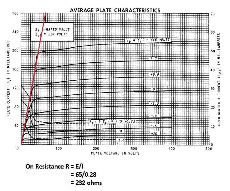
It looks as if I was justified in choosing a switch with a resistor in series for my simple model above. I will return to this, and then I will try to stick to this century’s technology.