36 Class C Part 3 Feedback around Modulator
The story so far:
I have investigated the idea of a “Class C” amplifier and pushed the notion that the feature that the active device conducts for less than half the cycle is not definitive. It seems much more important to dwell on the high efficiency amplification without regard to distortion, and then recovery of the wave shape afterwards. In AM or CW transmitter service, the recovery is carried out by a high Q tuned circuit called the “Tank Circuit.”
Although possibly not available to “old time” circuit designers, the idea that a high efficiency active device that is working as a switch, could be modulated with pulse width modulation seems attractive. Unfortunately a very simple modulator that gives pulse width proportional to signal gives a distorted amplitude modulation envelope.
Here is the waveform that I obtained when I modelled a circuit consisting of these stages:
1. Pulse width modulator
2. Switching Power Stage
3. Tank Circuit
4. Diode demodulator.
The brown trace is the modulating waveform, and the blue trace is the output from the demodulator. Note that the blue trace is much “broader” on the positive excursions than on the negative ones.
See my Post “35 Class C part 2”.
It was evident that the simple law chosen for the modulator was not right for the characteristic of the tank circuit in changing pulse width back into sine wave amplitude. I suggested two remedies. The first, was to put negative feedback around the whole modulator – power amplifier – demodulator system: the second was to design a pulse width modulator that varied the pulse in a way that would give the correct result at the Tank Circuit.
Today’s post is to explore the first: Negative Feedback.
Here is my model circuit:
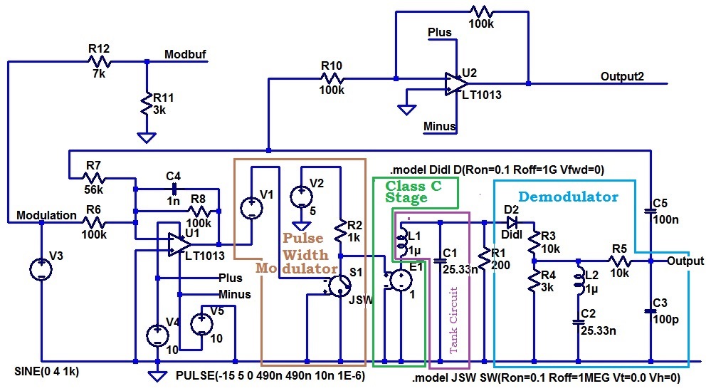
The demodulator is the diode demodulator we saw in the last post. I mentioned then that I added L2 in series with C2 to make a trap as I wanted to reduce the carrier, but did not want to put filter poles where they would interfere with my feedback loop. Notice the resistive divider R3, R4. This reduces the asymmetry that one gets if a shunt capacitor is placed directly on the cathode of the diode. In such a case, the diode charges the capacitor quickly, but it will discharge much more slowly. In this circuit, C3 and C2 are charged and discharged with much more similar resistances.
That’s the logic of it anyway. Probably completely invalidated with the addition of the series LC trap. Maybe diode demodulators is a subject for another day.
The resistive divider on the Modulation signal giving the signal Modbuf is just there so that we can see an input signal and an output signal that are similarly scaled.
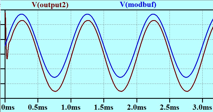
Here are the traces.
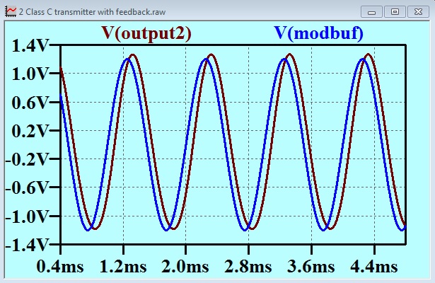
It is easy to see that the output signal is very much less distorted than without the feedback. As the output waveform is not created with a continuous process (the pulse width modulation), I cannot simply run a spice FFT on the output to measure.
I calculated the phase shift of the base band signal as it found its way along the forward path. The actual amplitude modulation of the carrier at the tank circuit is lagging the modulating signal by about 2.2 degrees. The output of the demodulator is lagging the modulating signal by 30 degrees.
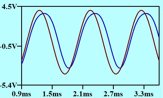
I tried substituting a synchronous peak detector for the diode detector. This effectively gave me a sample and hold on the peaks of the full wave rectified modulated waveform. This gave me a minimum ripple and enabled me to reduce the low pass filtering required for a smooth baseband signal. The result is shown below. You will see that the brown trace (output of demodulator) lags behind the blue trace (modulating signal) very much less with the synchronous demodulator.