In the last post I mentioned that we are so used to “Op Amp” thinking these days that we take some big simplifications for granted. An example is the output resistance of the op amp being very low. This resistance will usually break with stray capacitance at some frequency way out where we don’t care. In an example I looked at last time, we had a single stage exhibiting a two pole response. Of course the single stage (a BJT, say) will exhibit an output resistance that is not much lower than the collector load. It might break with stray capacitance at a frequency not too far removed from the frequency at which the input capacitance is having its impact.
Further on in ADALPAD, (pp 780 in Chapter 14 “Amplifiers with Multistage Feedback”) there is a two stage amplifier.

This circuit, or one very much like it, was promoted in “Radio and Hobbies” magazine when I was a high school student. I remember wondering at the time why two different transistor types were specified, when the duty seemed to be within the capabilities of either type. Looking back after all these years I would have to say that I suspect that the Radio and Hobbies people would not have known the answer.
The caption to the circuit in ADALPAD reads:
Fig. 14.35 Circuit diagram for an audio-frequency current -feedback pair. The gain is about 75, and the bandwidth about 8 Hz to 200kHz. OC44: alloyed germanium transistor, ΒN =60, fT = 10 MHz; OC71: alloyed germanium transistor, ΒN = 40, fT = 500 kHz.
Further down, the authors write:
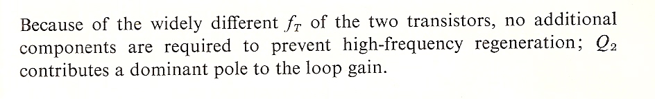
It all makes sense now. Note that as the feedback is taken from the second transistor emitter, the collector is not in the feedback loop, so stray capacitance on the collector will have little impact on the feedback loop. It is interesting that in those days a designer could choose transistors with confidence that their fT values could be in a known relationship. Maybe in those days the transistor manufacturers had a lot of trouble getting a specified fTand were selecting transistors for a specific “fT bin”. I don’t think that we could do that these days. My impression has been that transistor manufacturers generally specify a minimum value for fT and no maximum. I did a quick Google search on available data sheets and made up this table.
What the data sheets tell us about fT
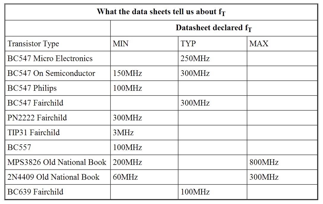
My quick Google search yielded only one transistor for which a maximum as well as a minimum for fT was specified, and they are an octave apart. I have a very old transistor data book which I keep because it provides much more data about transistors than is generally available these days. (National Semiconductor Transistors 1973) That book does specify some transistors where both a minimum and a maximum value for fT is cited. Note that the min and max are at least 2 octaves apart. This data does not provide for precise placement of poles in the transfer function of an amplifier design.
Come to think of it, have you ever seen a Maximum as well as a Minimum for the gain Bandwidth product on an Op Amp data sheet?
I think that circuits of the type depicted above are just not possible with today’s parts. One would have to place a capacitor somewhere to get one of those poles way below the other.
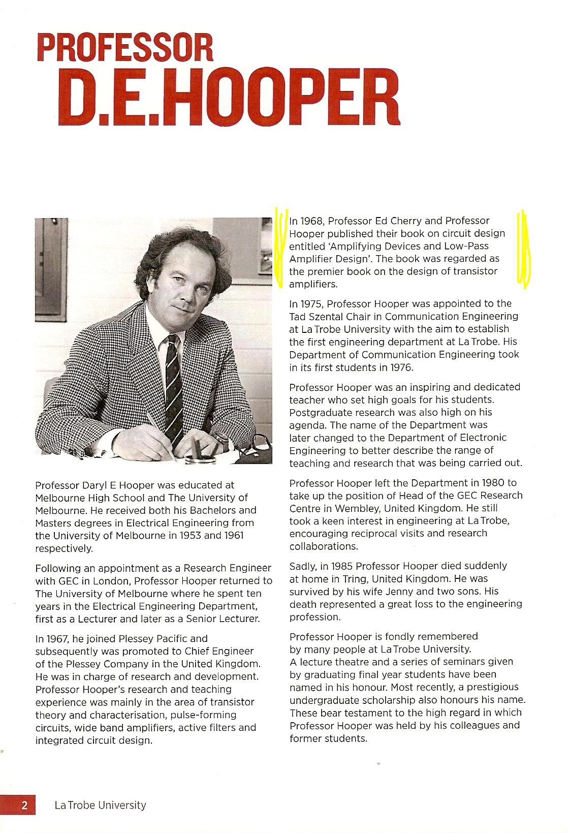
In November, I attended the annual “Student Projects Showcase” of the faculty of Science and Engineering at LaTrobe University. This is the department that was set up by the Hooper of ADALPAD. In the program for the evening, there was a little spiel about Daryl Hooper and I was pleased to see that mention was made of ADALPAD. I wonder how many of the 2012 students had read it.