In “Class C part 1”, I wrote about a discussion I had had with the designer of a low powered AM broadcast transmitter. That was Brian Cabina, who I had met through the Music Broadcasting Society. Must have been in the early 1970s. By the time that society began transmitting, the FM band had become available, but during early planning, it was proposed to utilize the AM band. New frequency allocations were being opened up (One was taken up by 3CR, for instance), and it had been hoped to grab one of these.
He had told me that with an amplitude modulated Class C transmitter, one had to put the modulator on the output of the last stage “because with Class C there is too much distortion”.
AM Transmitter with modulation of the power to the Class C output stage
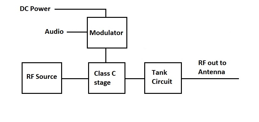
There is a heavy price to pay, as a portion of the power for the RF power amplifier has to be provided by an audio amplifier. This was expensive power, both in terms of capital cost, and in terms of efficiency.
I suggested that the blanket statement “with Class C there is too much distortion” is nonsense, and asked the rhetorical question “Can I justify that”?
My justification is that there are two completely independent avenues for distortion in a Class C transmitter and to blur the distinction between them, by grouping them under the heading “the distortion” is to prevent precise discussion.
Here are the two distinct distortions defined in a way that in my mind are clearly distinct.
Distortion 1.
This is distortion of the RF carrier in the Class C amplifying device. This distortion is removed (more or less) by the filter on the output. In traditional AM transmitter (or CW transmitter, for that matter) practice, the filter takes (took) the form of an L-C tuned circuit called the “Tank Circuit”.
Distortion 2.
This is the distortion that would be introduced in the audio channel between the input to a small-signal modulator on the input to the Class C stage, and the audio channel as it appears in the form of amplitude modulation on the output.
Distortion 1 is generally gross distortion indeed, and if that magnitude of distortion were to appear as Distortion 2, then that would certainly disqualify the circuit for serious AM work. However, Distortion 2 is either not related at all to Distortion 1, or related so loosely, that we can address Distortion 2 without regard to Distortion 1 at all.
If we were to modulate the signal at the input to a Class C stage, so as to achieve linear amplitude modulation of the output carrier, then what form should that modulation take? Not amplitude modulation. The Class C stage earns its stripes for efficiency by behaving as much like a switch as possible. The active device is either “on” and exhibiting as low a resistance as possible, or it is “off” and (in the instant) looking like an open circuit at the output. An exception that is possible, but divergent from traditional practice is that either one output device is “on” or another is, so between them a low resistance is presented to the output at all times. (See “Tuned Circuit with Voltage Drive” in the last Post “34 Class C Part 1.)
This is much more obvious to us these days now that we are familiar with switched mode power supplies, than it was to many armchair philosophers who contemplated Class C circuits in years past.
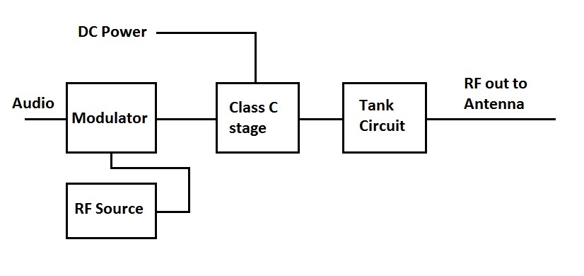
AM Transmitter with Low level modulator that modulates the signal to the Class C Stage
Our driver circuit modulator must maintain the signal amplitude to maintain the output stage efficiency. This leaves only one choice, the modulator must be a pulse width modulator.
This raises two questions.
Question 1.
If our transmitter block diagram has a small signal pulse width modulator followed by a Class C stage, is it possible in principle to provide an overall low distortion path to the audio.
Question 2.
What are the implications for the Class C stage of driving it with a signal of varying pulse width?
Let us go back a bit…
The tuned Circuit with voltage drive that I suggested in the last post was not really practical in “valve days” as the tuned circuit circulating current all passes through an active device. Any tuned circuit that was pitched at such a high impedance that the on resistance of a valve would not impose too much damping, would have much too much voltage swing for the valve to survive.
The huge differences between the old and new technologies are so obvious, that we don’t often bother to put numbers to them. Let us do just that in this case.
A 6V6 beam Power tetrode has a peak anode volts rating of 1200 volts, and a maximum anode current of 105 mA . The data sheets did not cite an equivalent of “RDSon”, but I estimated this graphically in the last post as 232 ohms.
An IXTP3N120 N channel MOSFET available at the one off price of AUS$13.461 from Element 14 has a maximum drain current of 3A and an RDSon of 4.5ohm. To get this low on resistance with 6V6s, we would have to have 52 of them in parallel. The change from one technology to another has not just made a change of degree in some parameters, it has of course made a change that has made completely new circuit arrangements available to us. This is blindingly obvious when we think about circuits such as switched mode power supplies, but it applies to Class C, RF power amplifiers as well.
These days we might search in a particular area of our “concept space” for a high efficiency design, and find a good result. That very same area was disqualified in the “valve days” on the grounds of heater dissipation alone. (The heaters in 52 6V6s dissipate 147 watts) In the real world 21stcentury, we might choose a different voltage range (lower), a different current range (higher) and a different value for “on” resistance of the active device(s). We choose these on their merits, rather then matching the performance of a huge number of 6V6s in parallel.
A Class C stage, which you might remember, is characterized by me (if not by the rest of the world) as one in which the (an) active device “is driven so as to provide a switching type of waveform without regard to distortion, and then the signal is recovered from the harmonics by a high Q tuned circuit called the Tank Circuit.”. Such a stage can be built around what I called the “Tuned Circuit with Voltage Drive” in the last post. Here is the model circuit again as a reminder.
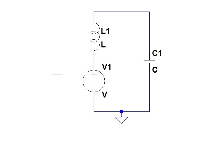
In this (what an old colleague of mine would call a) circuit topology, the circulating current in the tank circuit all passes through the active device(s) in the voltage source. Internal resistance in the active device(s) will be in series with the L and C. This is only practical if the internal resistances are very low. This is the case with (for example) MOSFETs with a circuit like that in a switched mode “half bridge”.
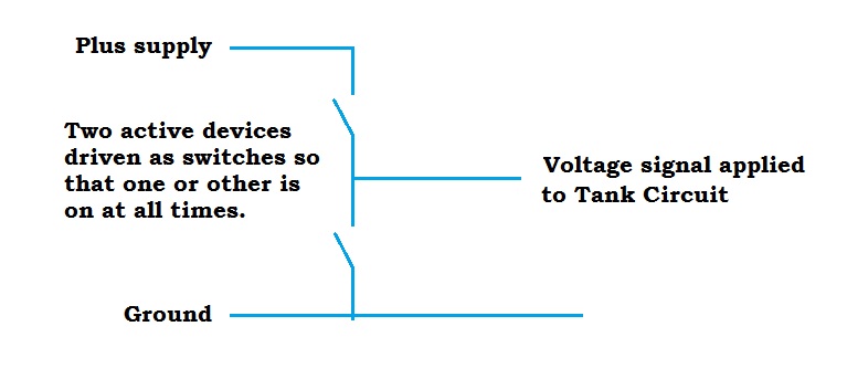
Here is an amplifying stage put together along these lines.

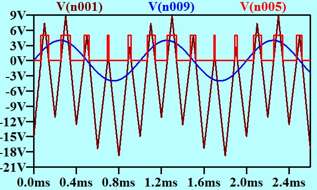
We start off with a source of signal at the carrier frequency. This is squared up with a trigger (which the RF boys (and girls) would call a limiter(?)) which I have implemented with a spice switch element. This converts the signal into a train of pulses which drive a complementary pair
The spice switch model has an “On Resistance” parameter, which I have set to 0.1 ohm. This accounts for the distorted nature of the waveform at the output of the power stage. This output has to carry the large sinusoidal current in the Tank Circuit.
The very output, the voltage imposed on the load resistor R1, is a sinusoid with low distortion, which we might regard as a recreation of the waveform on the input to the amplifier.
This “topology” which one might regard as an implementation of the “Tuned Circuit with Voltage Drive” ideal, will appear in several examples to follow.
MY definition of “Class C” includes the concept “ without regard to distortion”, and this is embodied here. The signal for exciting the Tank circuit becomes a train of pulses, and then is returned to a sinusoidal form by the Tank Circuit itself. Is this the distortion that I was warned about when I was a youngster? It is what I defined as Distortion 1. above?
What are the implications for Distortion 2 (the distortion of the modulating signal) of my practical implementation of “Tuned Circuit with Voltage Drive” topology?
Let us investigate this.
There are really only two ways we can apply modulation to the train of pulses at the output of the limiter. One is to modulate the amplitude of the pulses, and the other is to modulate the width of them. A moment’s thought will reveal that the modulation of the amplitude of them, amounts to the varying of the voltage source V1 in my circuit model above. This is the ordinary old modulation at the output of the RF amplifying stage, with the attendant disadvantage that some of the power to the output stage has had to come from an audio amplifier and is expensive power.
Pulse width Modulation of the Drive to a Class C Output Stage
Here is my first crack at a model to demonstrate this:

The pulse width modulator is set up to modulate the carrier with a 1 kHz sine wave. This is done very simply by adding the modulating sine wave to a triangle wave at carrier frequency and then passing the sum to a zero crossing detector. I have demonstrated this with the waveforms below in which I have reduced the carrier frequency to 5 kHz so that the carrier waveform and the modulating waveform can both be seen clearly on the same axes.
Here the blue line is the base band signal. The brown trace is the blue line with a triangle at the carrier frequency added to it. The triangle has the same slewing rate on the positive and negative going slopes. The red trace is the output of the zero crossing detector. This arrangement of pulse width modulator has pulses that are centred in a periodic fashion. That is the fundamental of the fourier series does not have phase jitter. This pulse width modulator has pulses with a width proportional to the voltage of the baseband signal. Is that the right characteristic in this case?
In this model, I have represented the power output active devices as a spice model voltage follower. You will understand that the circuit models that I present here have been placed in an order that has, I hope, a logical pattern to it. This is by no means the order in which the models were created. During the evolution of each model, there have been several steps that we will not bother with here. It just means that changes crop up from model to model. Generally, I won’t comment on these if they have no impact on the argument.
A simple diode demodulator is used. The introduction of L2 in series with what had been a low pass capacitor C2 to make it into a trap, had been done at some stage to reduce the carrier ripple on the output. I wanted a clean recovery of the baseband signal without placing a pole too low. This was my quick “no thinking” solution, which suited me in the moment better than a multi-pole filter.
Here is the base band modulating signal and the output on the same axes.
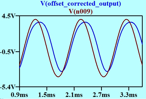
The brown trace is the modulating signal, and the blue trace is the output of the demodulator. Considerable even-order distortion is evident. Is this the distortion that I was warned about all those years ago, that I have identified as Distortion 2?
It can possibly be seen more clearly if the base band signal is replaced with a linear ramp.
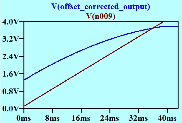
Here the modulating signal is a trapezoidal wave of low frequency. Here we look only at the rising edge (brown trace). The blue trace is the output of the demodulator.
If this is Distortion 2. then it seems pretty benign to me, and aught to be amenable to a little fixing with negative feedback.
Then again, and this is a possible second approach, maybe the “pulse width proportional to voltage” is not the correct transfer function for the pulse width modulator in this application. Maybe a modulator designed with a little more care would fix this distortion.
These two approaches – negative feedback, and smarter modulator – will be examined in the next post.
By the way, I am aware that conventional Class C circuits are not amenable to pulse width modulation. I suspect that the tank Circuit would have to be re-tuned every time the pulse width was changed.
Here is a “modern” (solid state) schematic for a Class C transmitter that I found on the internet.

Aren’t RF designers funny people! It seems that the active power device is also performing the role of limiter (approximation to zero crossing detector). I interpret the FD700 diode between base and emitter as being to provide a symmetrical non-linear load for C1 so that the transistor can be driven hard on positive excursions. Why don’t RF designers have to worry about transistor saturation? You can see that the reactance of the RFC is in with the Tank circuit when the transistor is “off”, but not when it is “on”. This circuit could not be used with pulse width modulation as the Tank Circuit tuning would be adversely affected.