The story so far:
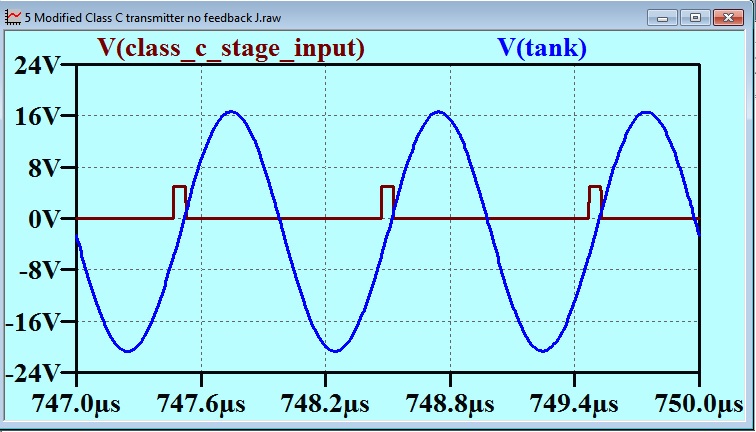
After proposing pulse width modulation of the input signal of a Class C stage to determine the amplitude on the output, I showed that if we used a simple pulse width modulator that varied the pulse width in proportion to the instantaneous value of the baseband signal voltage, we got a distorted result.
I postulated two approaches to fixing this in Post 35. The first was negative feedback and the second was “smarter modulator”. I showed how effective feedback can be in Post 36. Now we turn to the “smarter modulator”.
The short version is that the output (in real life – high powered) tank circuit is mimiced with a low voltage LC circuit. This circuit is fed with a variable width pulse to maintain the amplitude close to that of a reference signal obtained by amplitude modulating a representation of the carrier with an analogue multiplier.
I will provide particulars and then show the result.
Particulars
There are two steps.
First, the carrier signal is processed to generate various special signals that are required by the modulator proper.
It will be easier to find what follows clear if it is remembered that the tank circuit has the property that the quasi sinusoidal on it is placed so that the driving pulse falls on the positive going zero crossing.
The first signal generated is a signal I call “dual_slope”.
The signal has a notch shape that is centred on the positive going zero crossing of the carrier.

This could be generated in any number of ways. If you are interested, this is how I did it.
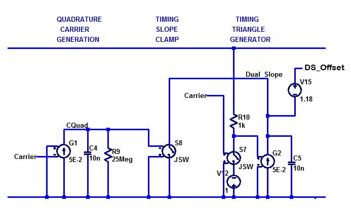
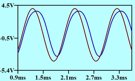
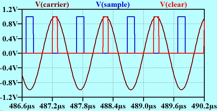
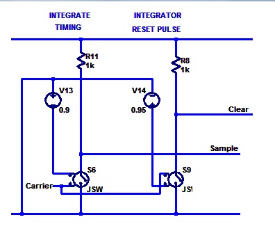
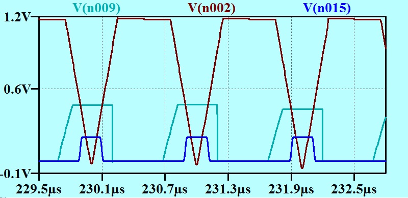
The second is a pulse “Sample” that occurs during the time when the carrier is near the most negative value. This pulse is accurately centred on the time when the carrier is at exactly the minimum value. See the blue trace below. The third is a pulse of less critical timing “Clear” that occurs later.
As before, I won’t go into the details of how these pulses are generated, but will show my model schematic for those interested.
The only other signal required for the modulator is a representation of the amplitude modulated signal that the Class C stage is to produce. Of course in this low level signal modulator board, this is easy to do with an analogue multiplier IC.
Second Step
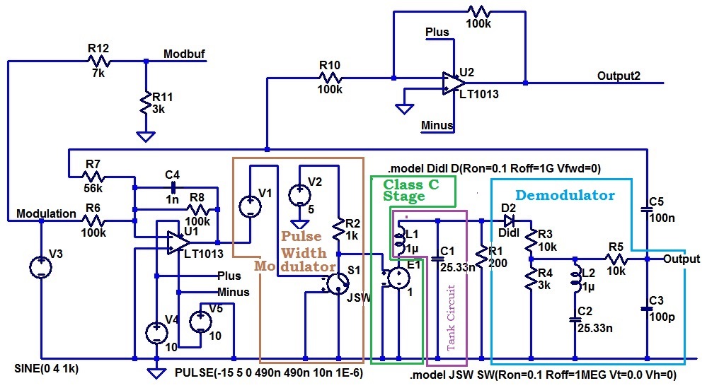
Now we come to the actual Pulse Width Modulator for Low distortion Class C stage.
It is easiest to describe the operation of this when it is already running. It is easy enough to extend this to graceful start-up. I will leave that to the imagination of the reader.
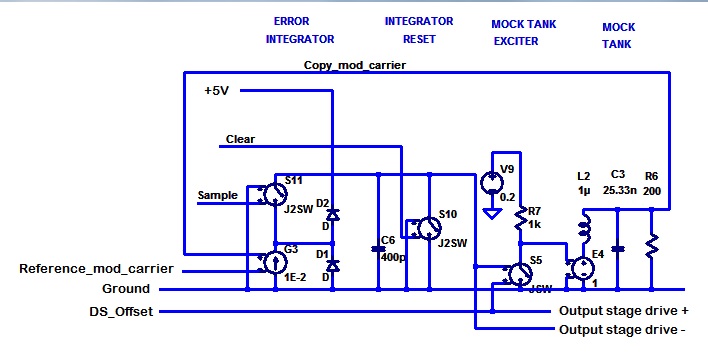
To the right of the circuit diagram there is a tank circuit and an exciter arranged just as I have arranged these in previous Class C stage models. The idea here is that these are all small signal components on the “modulator board”. It has appeared later that there might not be any reason for this “Mock Tank Exciter” and “Mock Tank”, as the actual exciter and tank could play the role here. I will leave this as it is for this explanation.
The voltage on the Mock Tank is compared with the modulated signal from the analogue multiplier at the voltage controlled current source G3. This then provides a current that is proportional to the difference. This current is shunted away by diode D1 or diode D2 except when the voltage controlled switch S11 is closed during the “Sample” time.

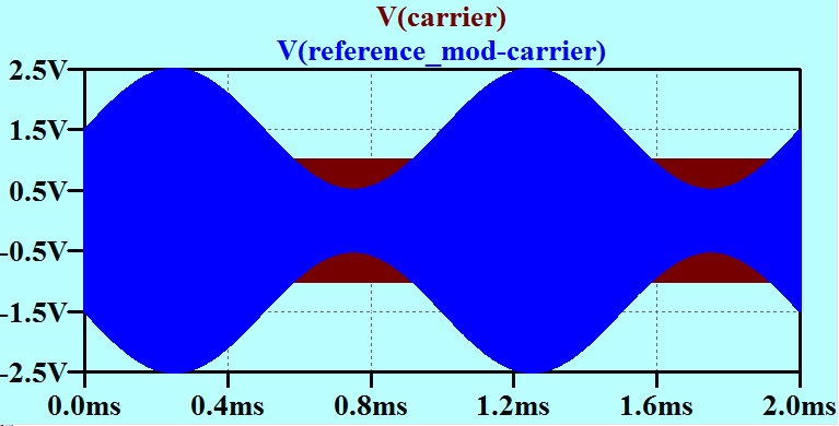
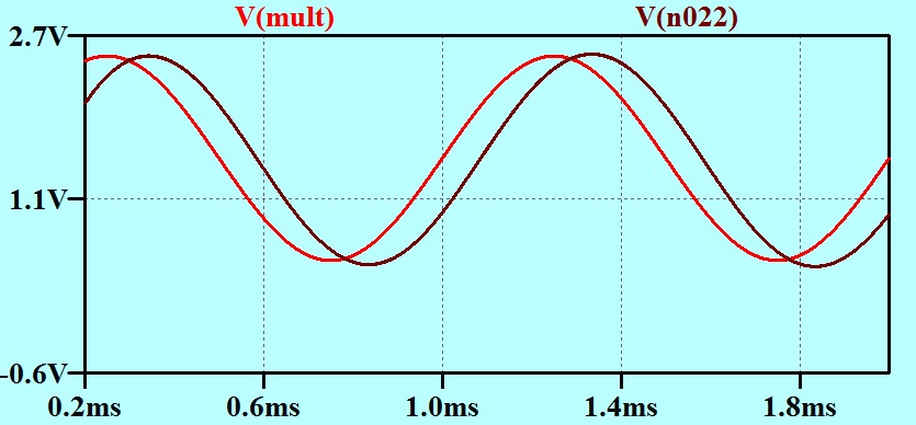
The voltage on the Mock Tank circuit is the brown trace. The reference modulated carrier is the blue trace. It will be seen that the magnitude of the reference modulated carrier is greater at the negative excursion. During the Sample time (red trace) the current representing the difference is used to charge capacitor C6. At the end of the Sample pulse, the charge on C6 represents how much the Mock Tank circuit is falling behind the reference signal. This is then used to determine the duration of the pulse of energy imposed on the tank by the exciter in the following cycle. C6 is discharged on the Clear pulse (not shown) The voltage on C6 is converted to a width of a pulse that is properly centred so as not to introduce phase modulation by comparing it with the dual_slope signal.
Here the DS_Offset (Which is “dual_slope” with an offset added) is shown in brown. The voltage on the capacitor C6 is green as before. The blue trace shows the excitation signal for the Mock Tank. It is high whenever the C6 voltage is higher than the voltage of “dual slope”. It can be seen that this scheme will provide a variable pulse width to excite the tank, and that the width will vary as required to provide just enough energy to the Mock tank to have its voltage fall just a little behind that of the reference signal. At the same time, the driving pulse is properly timed so that there will be no phase variation as the amplitude is modulated.
I am writing this up many weeks after I developed the model. There are various reasons for regarding this as unnecessarily complicated. The complication would all be accounted for in a very small board area of small signal circuitry, so would be readily born if it gave the best result. What result does it give?
The red trace is the base band signal at the very input to the model.
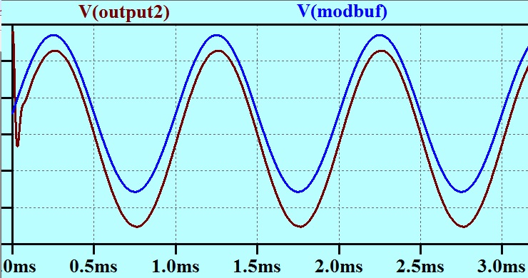
The brown trace is (with attenuation and offset) the output of a synchronous demodulator on the high powered tank circuit.
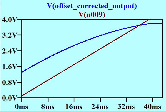
One way to check for linearity is to modulate with a slow ramp and look for the straightness of the ramp on the output. here is what we get.
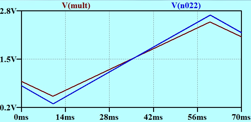
The brown trace is the input to the modulator, and the blue trace is an attenuated version of the output from the demodulator. That is linear!
Compare this with my initial “crude” pulse width modulator in which the pulse width is proportional to the voltage.