There has been a delay of many months in getting this blog post out the door. This has not been because of flagging interest, but the opposite: there have been interesting revelations and discoveries that have caused the goal posts for this write-up to move about. Several times, I had thought that this post was complete, and then new information came in, or a new insight was gained that seemed to redefine the problem.
The factors that have come to bear, fall (in part) outside the scope of this blog, as I have tried to keep this blog focussed on the technical aspects of electronic engineering. The subject of how to order the affairs of an engineering team for synergistic productivity has been kept aside for publication in a different forum. However we can never really divorce the consideration of how we design something from the consideration of how that design task will fit into an overall plan.
I will touch lightly here on one aspect of project management that has had an impact in this case. This is risk management. Almost by definition, until some development work has been performed, we do not know what the outcome will be. If we knew the outcome in every detail, there would be no development work to do. One possible path through the development work is that a design approach is thought up and documented sufficiently for a prototype to be made. Testing of the prototype will yield results that might:
(a) Prove that the idea is without flaw and can be incorporated into the design without modification.
(b) Show that the idea is workable, but that changes have to be made in breathing life into the prototype. These changes might represent a discovery that there was a mistake in the concept, or a mistake in the documentation that served to represent an invocation of the concept.
(c) Show that the idea is not suitable to proceed with.
Of course, one hopes for an (a), but one has to be prepared to proceed with the project whatever the outcome of the prototype building and testing (the “technicianing”) effort.
Note that if no competent technicianing effort is brought to bear, then the conclusion will be that we have a (c). This might be an error, and a really good (a) or (b) opportunity can be missed.
It falls to the project manager to conduct realistic risk analysis before the technician sets to work, and to have plans up his sleeve for all outcomes. Part of his work is to evaluate the competence of the technician workforce. If the technician assigned cannot distinguish between a failure on his part, and a failure of the concept, then a different plan is called for.
During explorations with spice during the preparation of this blog post, I discovered a simple mistake in a concept implementation that I had made in 1987. [Spice was not available (to me) at that time. The first implementation of spice that stepped out of the mainframe/Fortran environment seems to have been released in 1985. (See here.) Another reference says 1989, but it looks as if that can’t be right. James Fenech has a “Pspice” book that is dated 1988. In my next job, (1988) I was using MC3, an early schematic entry based spice invocation.] The mistake was immediately obvious, and very easy to fix. It would have been very obvious, and easy to fix by the person charged with the task of getting the prototype going in 1987.
The concept described in this blog post was wrongly categorized as a (c) in 1987 by the team technician and my boss. A big mistake.
Here we go then:
My second example of the exploitation of the relationship of two frequencies in the ratio of 2.5 to 1 is also a communications one.
The application was a network of stations that were to be linked by radio. There was one central station which was to gather information from all the others. Some radio links were short and could be expected to provide a strong low-noise signal at the receiver. Other links were longer or involved difficult paths, and were expected to present a noisy or degraded signal at the receiver. We were aware that it would take more time to send an error free packet of data down a noisy and degraded link than through a high fidelity one.
The amount of traffic was such, that it looked as if we could not slow the traffic down on all links to meet the needs of the worst one. We needed a system with a variable bit rate. The rate on each link could be set at commissioning time, or (and this was my hope) set dynamically to adjust to the needs of each link. Dynamic bit rate adjustment might require expensive or tricky software. We did not have any idea of an algorithm for it. It looked as if “set up” bit rate for each channel would be workable, if not complying with all my flights of fancy.
Many readers in this forum know the difference between bit rate and symbol rate. For those who are not quite clear on this, here is a brief diversion.
The symbol rate, for which the unit is the baud, (pronounced “bode”) is the rate at which data are passed. Each datum, however can carry more than one bit of information. The number of bits per symbol need not even be an integer. Imagine a channel that transfers equally likely symbols that are a number between 0 and 9.
Number of choices, N = 2n where n is the number of bits.
n = log2(N) = ln(N)/ln(2)
= 3.321928
At first, it might look like a really difficult problem to deal with symbols with that number of bits each, but it is in fact very easy.
1. Look at the first symbol
2. Get the value of the symbol.
3. Multiply by 10
4. Add the next symbol symbol
5. Loop back to step 3. until the end of the message is reached.
I first encountered a simple and practical application of a non-integer number of bits in the Digital Equipment Corporation Radix-50 system. https://en.wikipedia.org/wiki/DEC_Radix-50
In this system, characters were drawn from a character set of 40 characters
(space, A, B, C, D. E, F, G, H, I, J, K, L, M, N, O, P, Q, R, S, T, U, V, W, X, Y, Z, $, ., %, 0, 1, 2, 3, 4, 5, 6, 7, 8, and 9). Forty is “50” when expressed in Octal, the preferred numbering on DEC machines; hence the name. The number of bits of information embodied on one of these characters is 5.3219 (or thereabouts). Packing three of these characters into a 16 bit word is very simple.
(using decimal notation)
The characters are assigned values from 0 to 39
Take the first character and multiply its value by 40
Add the second character.
Multiply the sum by 40
Add the third character.
The maximum value of the result is 63999. This is less than 65535, the maximum value we can store in 16 bits (binary 1111 1111 1111 1111), and will thus fit in a 16 bit word.
Extracting the characters is easily accomplished by dividing by 40 a couple of times and saving the remainders. All this was worthwhile in the days when non-volatile memory was made of magnetic cores, and a 32k x 16 memory board was a big expensive memory!
In a variable bit rate system, it is a simple matter to vary the multiplier to suit the number of choices represented by the symbols in each link.
[Note that we might regard this as an extension to the simplified concept we apply when we say (for example) that an LS74374 is an eight bit register. We say this without regard to what information it might hold in any particular implementation. If it only ever holds the ascii representations of the numerals 0 to 9 then there is a sense in which it is a 3.321928 bit register. The use of bit is thus context sensitive. I have never seen this lead to ambiguity. There is a third level of sophistication that we could apply when we consider the probabilities of occurrence of the particular values (following Shannon). The communication system being described here employed a layered architecture, and the layer being considered (lower layers) did not have information about the meaning of the data that was being handled, or the probability of occurrence of any particular values.]
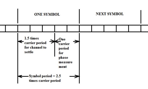
The data was encoded by phase shift keying a tone with a frequency that was placed in the middle of the baseband. This was 1650 Hz. The symbol rate was 660 bauds. The time required to set up the carrier with a new phase, and let the bandwidth limited channel settle and then measure the phase at the receiver end was just 2.5 times the carrier period.
The receiver was phase locked to a pilot tone with a frequency at the symbol rate, that is 660 Hz. The symbol time was divided up like this:
In this receiver the channel was gated so as to accept only the last two fifths of the symbol time. The gate period is exactly one cycle of the carrier frequency. The symbol data is determined from the timing of the positive going zero crossing during that time. This was done with a technique that I think I must have pinched from Ed Cherry’s “Omtrack” Omega receiver. An eight bit counter is clocked at 256 times the carrier frequency. When a trigger circuit detects the positive going zero crossing, the contents of the counter are transferred to an eight bit latch.
The pilot tone will add some error, although this could easily be corrected for by cancelling it out. In the first instance, (pilot tone 15 dB below carrier) we showed that the system would work without correction.

One task was the establishment of message timing at the receiver. This was a task for which an approach was proposed but several back up approaches were formulated in case there were problems with the first.
The proposed message format consisted of an initializing period during which a 660 Hz (symbol rate) pilot tone was transmitted at the maximum amplitude provided for by the channel. After sufficient time for the receiver phase locked loop to capture the message pilot tone phase trajectory, the pilot tone amplitude was reduced to a small fraction of the initial amplitude, and the receiver phase locked loop speed was reduced, as from then on it only had to correct for errors due to phase drift, a low frequency phenomenon.
I knew less about feedback loops then than I came to know later, and the provision I made for adjusting the speed of response of the phase locked loop (fast for acquisition: slow for phase maintenance) was very naïve by the standards of today. I used CMOS switches to select between two different loop filter alignments. Interestingly, I have seen that “naive” scheme published by others, so I was not the only one to miss an opportunity. Perhaps varying the speed of a control loop could be the subject for another blog post (but see below).
The interesting trick is that the gate circuit which passes the channel signal for exactly one cycle of the carrier, also forms the first block of a neat phase comparator for the phase locked loop that keeps track of symbol timing. This phase comparator has very good resistance to interference from the carrier. The signal from the gate is fed to an integrator. Over the one carrier cycle time, the net contribution to the charge on the integrator from the carrier is zero. The sample of the pilot tone, is however a measure of the phase error. The output of the integrator is captured at the end of the integrate time by a sample and hold circuit.
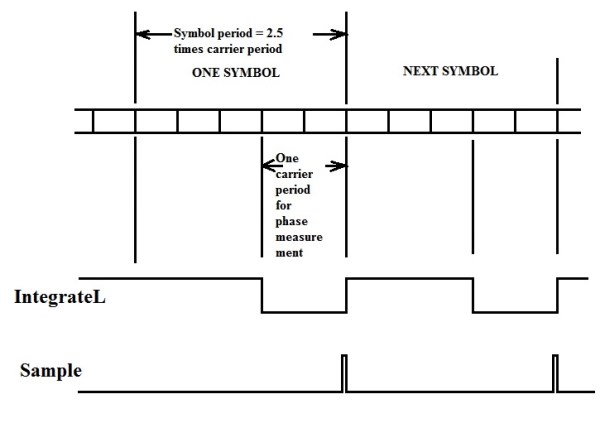
I have shown the narrow “Sample” pulse occurring right at the end of the integrate time. Of course, the integrate time could be brought to an end, and then the static voltage on the integrator sampled after that. Analysis showed that this was not necessary. The situation is analogous to an A/D converter following an amplifier with no sample and hold. If the slewing rate of the amplifier output is low enough, and the A/D is fast enough, the special saving of a static value is not required.

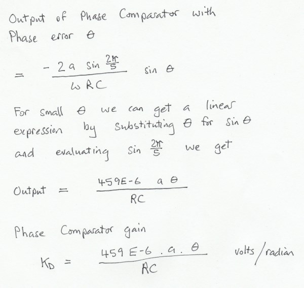
This is the block diagram of the “Carrier Immune Phase Comparator”.
For this phase comparator, we have:
RC is the time constant of the integrator.
Note that this expression has two components that depend on the pilot tone signal. θ is the phase error, and a is the amplitude. If we like, we can represent these as being introduced to the loop separately. That is, we can take a out of KD and apply it to the loop separately.
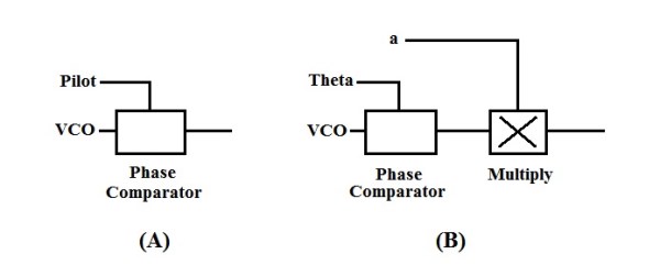
You can see that the (B) block diagram representation is the same as the (A) representation, except that the θ and the a components are shown separately. This clarifies an interesting point. There is a multiplier in the loop, and the loop gain depends on the amplitude of the pilot tone.
Here I show a “canonical” phase locked loop representation on which I have added the signal names from the discussion above.

If the loop filter has a characteristic which has falling gain with increasing frequency (which it will inevitably have), then the speed of the loop will change as the loop gain changes.

Here I show an arbitrarily chosen loop filter characteristic. The brown line represents the loop gain that we would have during the initializing period when the pilot tone is at full strength. The blue line represents the loop when the pilot tone has reduced by 15 dB during the data transfer part of the message. This means that a has reduced by a factor of 0.178. Note that as the loop gain is reduced (Arrow 1. on diagram), the unity gain crossover frequency is reduced (Arrow 2. on diagram) by a factor of 3.2/16 = 0.2 (which is about 2.3 octaves)
The red line is the pilot tone frequency.
I was very pleased with this phase comparator concept, although these days, I would approach that original problem very differently. It seemed to me that the line of thinking behind this phase comparator might have other applications, and indeed this has been the case.