Author Archives: admin

Fuses 2

I have had some interesting correspondence since I first posted on the subject of Fuses. One correspondent used to be a designer of HRC (High Rupture Capacity) fuses for switchboards. He wrote to me (in the face of the wonderings that I expressed in the last post) that the use of the fine silica sand is a constant, and that the various fuse characteristics are obtained by the design of the metal element. Interestingly, another correspondent used to be a designer of the sort of fuse that you see on a power pole. In that environment, it seems that special care it taken to design a fuse that will behave satisfactorily when there is a sufficient current to make the fuse very hot, but not (in the short term) enough to open it. A red hot fuse would be the sort of thing that would start a bushfire. Apparently in that environment an interesting innovation is to use boric acid rather than silica. Of boric acid, Wikipedia says:
Boric acid, also called hydrogen borate, boracic acid, orthoboric acid and acidum boricum, is a weak acid of boron often used as an antiseptic, insecticide, flame retardant, neutron absorber, or precursor to other chemical compounds. It has the chemical formula H3BO3 (sometimes written B(OH)3), and exists in the form of colorless crystals or a white powder that dissolves in water. When occurring as a mineral, it is called sassolite.

Obviously, even in the simple case with a silica filled fuse, the silica has a role to cool the element before it opens and to cool the plasma once that forms. These effects will obviously vary with temperature. In the world of heavy current fuses, I am informed of the following: “It is a common misconception that the fuse will eventually blow at the rated current.  If you look closely at most fuse characteristics the minimum melt time asymptotes toward infinity at about twice the rated current.   The reason for this is that the rated current is usually the maximum current the fuse can carry without being damaged.  So if you have a 50A rated fuse, it will happily carry 50A from now till eternity.  Given rating tolerances, which tend to be minus nothing/plus something, it will probably carry more than 50A with no ill effect.” Is this the case with small fuses of the type and style that we might install on a circuit board? Here is a set of graphs from a LittelFuse catologue.

  The 1 Amp curve does seem to be at about 2 amp at the 100 second line. This is somewhat quicker than “till eternity”. It looks as if we need to look carefully at these details for each special case. The extremes are easy. The “Fuse Survives” and “Fuse opens promptly” regions seem pretty clear, but there be dragons in the middle there. Often in electronic circuits, a fuse may be desired, yet unless special measures are made, there might not be sufficient fault clearing current to open the circuit promptly. The use of a dirty great SCR as a crowbar used to be popular. The SCR can be triggered by either excess current, excess voltage, or indeed, any other fault condition for which we would like to open the circuit. In cases where we do not want to add the expense of a crow bar, we might nevertheless want to minimize the problems caused by dithering around in the badly defined region. Some circuits can make this situation worse. Here I will tell a story against myself. I had a design in gestation, and the client wanted a fuse added. The addition of a fuse was not to protect against any particular perceived fault condition: it was just that the existence of the fuse was going to add to the client’s sense of well-being. Here is the power supply part of the circuit that I drew up at the time:


(Hey you young blokes, don’t knock my drafting! This was drawn 2 years before the Protel (Altium) company came into existence!)

All three of the three terminal regulators have output current limit, and over temperature shut-down. Thus they rather protect the fuses from short circuits or over current faults down stream. It seems a bit silly now to spend time trying to justify details of a circuit that dates from 1983, but I suppose that if one of the regulators has a melt-down, we want to protect the power transformer from being cooked.

A big problem here is that the fuse is carrying the bridge current, and the regulator is drawing DC current from the res cap. As is well known, the RMS current at the rectifier is higher than the DC output current with such a circuit. I used to go by a rule of thumb that the RMS current was three times the DC current. Of course it all depends on the impedances in the curcuit, and how “spikey” the bridge current waveform is. Without worrying too much about the assumptions, I did a quick circuit model. Here is the circuit.

I have made all the resistances VERY low, and not included any leakage inductance in the power transformer at all. Refinement of this model could be for another day. The load current in the circuit ramps up to 10 amps. Here are the results:

In this low impedance, 10 amp output circuit, the results are:
With res cap value = 10mF, RMS current is 1.65 times the DC output current
With res cap value = 100mF, RMS current is 2.6 times the DC output current
With res cap value = 1F, the RMS current is 2.9 times the DC output current.

The capacitor values here are huge. These sorts of numbers would also be obtained with much smaller capacitors with a lower current circuit.

Thus if we have a design where the DC current to a regulator was 1 amp. we would need a 3.5 amp fuse at least. The problem is that with a regulator failure, the first thing that will happen is that the res cap will empty all its energy into the regulator without any damage to the fuse. The current in the regulator might then be (say) 10 amps. This is ten times the normal current, but the current in the fuse has only increased by a factor of about 3. The short circuit is a lower impedance than the res cap over the frequency range of interest, and the circuit is no longer acting as a peak rectifier. If a fuse from a family such as that represented by the curves above is used, it will open in about 20 seconds. Is that as fast as you would have thought for a ten fold increase in current to the regulator?

One of the experts told me that a problem with fuses of 10 A rating or less, is that they open very quickly. I made a quick attempt to model a fuse at the front of  a switched mode circuit to see what overvoltages I might see with such a high di/dt in the leakage inductances. In the time I could spare, I did not get the model to work. Mental note – watch out for this.

I designed a circuit similar to the one shown above, but the power supply had to supply a dot matrix printer hammer driver. I do not have a record of the value, but this circuit had a very large res cap to minimize the volt drop on a printer hammer drive event. I was watching the prototype during software testing, and noticed that the wire in the 3AG glass fuse was running red hot. I increased the fuse rating. I had wanted to provide hardware to determine the timing of the hammer drive pulse, but the client insisted on doing this in software on cost grounds. During testing, the software left one (or more) of the hammers on for an extended time. The circuit board tracks failed before the fuse did. This was 20 years ago, and I have always taken care with my fault scenario analysis since then.


Fuses

This post has only one ending, but it has many beginnings. There are various literary techniques for dealing with this, but I am not skilled in these. Let us just look at all these beginnings and see where that leads us.

One.
Back in the dark ages when I was at high school, probably about third form (now called year nine) there was an interesting event. In one of the science rooms some sixth formers were conducting an experiment. A glass rod was held about 500 mm above the bench with a laboratory clamp at each end. Near the middle, a wire was wrapped tightly around the rod in two places about 20 mm apart. My eyes followed the wires. This 20 mm of glass rod was wired to a power cord. It was in series with the mains and an electric jug. It seemed as clear as anything that the jug was not going to boil water, as the 20 mm of glass rod between the wires was a good insulator. The experimenters lit a couple of bunsen burners and proceeded to heat the glass rod. One of them explained to me that glass was a conductor at high temperature. I was sceptical, but hung around to see what happened. What happened was that a teacher arrived and saw the bare wires on a circuit that was plugged into the mains, and all hell broke loose! Fortunately this was one occasion when I was not in trouble. I made a discreet exit from the room, and that was the end of that, except I often thought about it. It would have been interesting to see that experiment completed.

That was then: this is now. Now you can see that experiment completed at Glass Conducts .

Two.
In the 1970’s I used to subscribe to a magazine called “Wireless World”. There really isn’t anything quite like it these days. There was a very wide range of contributers. Wireless world would print contributions that looked really crazy. In those days a frequent contributer was Ivor Catt who wrote articles to explain why he thought that James Clerk Maxwell and Albert Einstein were all wrong. Some years previously, Authur C Clark had put forward the idea of geostationary satellites in a Wireless World article. The magazine carried articles about audio equipment that ranged from the important to the wierd. In the first category were Peter Baxandall, Douglas Self, John Vanderkooy and many others. Many issues contained papers that one would want to keep, and I kept them.

Three.
A few years ago, I was doing some design contract work for Omnitron Technologies. Part of this involved revision of sparsely documented work done by others. In the design there were several instances of drive of a large MOSFET or IGBT through an isolation barrier. My predecessor had chosen an HCPL316J for this. You can see the datasheet here. This device includes a fault detection and automatic shutdown scheme, that Avago call “Desaturation Detection”. The saturated power switch pulls down a logic input through an external fast high voltage diode. The idea is that if a fault current arises, that will pull the switch device out of saturation. The rise in voltage is detected, and that initiates the shutdown. The detail that intrigued me is that is is a deliberately slow shutdown. The operation is described in the data sheet like this:

 And again, in the more detailed blurb:

Further down, details are provided.

The above extract from the Switching Specifications table does not show the units for the times. The unit is microseconds. Obviously the chip designers set out to respond to the IGBT being pulled out of saturation as quickly as possible, but then allowed 1.5 to 2.7 microseconds for the switch-off transition. Such a slow switching transition, if repeated every cycle in a switching circuit would give excessive switching losses. If it occurs only once, then the rise in IGBT die temperature is clearly considered a lesser evil than the excess voltage from the circuit inductance if the switch-off is faster. It is an interesting idea, and a surprising idea that a compromise switch-off speed can be found by the designer of the chip, who knows very little about what inductance might be in that fault current circuit. Leaves you thinking.

Four.
(Now we are getting closer to the actual subject of this post.) I write a column called “Sparks ‘n’ Arcs” for the magazine Australian Model Engineering. In the issue for July-August 2013, I covered the subject of fuses, and explained the significance of the I2.t measure. For your convenience, I have placed an extract of this article here. Copyright for my writing in that magazine is held jointly by me and the magazine. I have the magazine editor’s permission to make this extract available in this blog post. If you would like the whole article, that is obtainable by purchasing that magazine issue from the  AME Retail Shop.

(For continuity of my story, I suppose I am assuming you will be interested to read the article extract.)

Five.
I have been clearing out a lot of old stuff, and in order to make space (for new stuff) I am going through my old Wireless World magazines and keeping only the articles that I want, and discarding the rest. I just discovered an article “Fuses for the protection of electronic equipment” by R.A.W. Connor, F.I.E.E. He covered the basic material much as I had done in my AME article, but then introduced a thought that was new to me. It was new, but in a way, I had been drip fed vital bits of information since school days.

In many applications for an HRC fuse, there will be sufficient inductance in the circuit for an appreciable amount of energy to be stored before the fault is cleared. It falls on the fuse, then, to not only clear the fault current, but to dissipate the energy that the fault current has stored in circuit inductances. If the fuse opens instantly (an arc forms and then extinguishes) then the inductance might cause an over voltage failure of the very components that the fuse has only just saved from an overcurrent. The designers at Avargo who designed the HCPL316J could tell you that. I have read in many places that the powdered silica that an HRC fuse cartridge is filled with, acts to draw thermal energy from the arc and extinguish it quickly. R.A.W Connor has just filled in a critically important part of the story for me. The arc raises the temperature of the silica powder so that it conducts. It provides a shunt path both in the thermal sense and in the electrical sense. By shunting current from the arc, it promotes rapid arc extinguishing. Then the thermal mass of the rest of the cartridge full of silica powder comes into play and lowers the temperature so that the silica is no longer conducting.

Why hadn’t I grasped this before?

I wonder if the silica has different concentrations of salt doping for different fuse voltage ratings?

Load Line

In the previous blog, I generated a graph to show that a constant voltage active load driven by a high impedance source (in this case 240 volts RMS 50 Hz supply in series with a 3 Henry inductor) could establish one of two voltages to draw a particular power (in this case 18 watts). Here is the graph.

See the previous post for details. I really wanted to show this on a graph with current vs. Voltage axes, where the constant power line would be an hyperbola and it would cross the load line in two places. Here I set out to do this.

 Readers of this blog are likely to be familiar with the notion that the vector voltage across a resistor, and the vector voltage across a reactance in series, provide us with the wherewithal to construct a circular locus. In reflecting on this task, I have realized that in fact there are two different circles, and that we choose the one we want according to context. In small signal circuits, the reactance is most often a capacitor, but an inductive reactance shares the same critical property: the vector voltage is at right angles with the vector voltage across a resistor in series. Consider this circuit:

The voltage across the resistor, VR and the voltage across the capacitor VC add to give the input voltage Vin. (Kirchhoff, or something, isn’t it?) Vectorially, the addition of voltages can be represented thus:

As we learned in high school maths, “The angle in a semicircle is a right angle”. This vector (phasor) diagram is lovely to reflect on. It does not matter what the relative proportions of VR and VC are, the radius (shown dashed) of the circle to the point of connection between the vectors is constant. The relationship between the proportions of the vectors might vary with frequency as the reactance varies with frequency: here we have the genisis of an all-pass filter. On the other hand, if the radius is held fixed and at right angles to the input voltage by feedback, we have half a bridge that might form the basis of an audio oscillator.

I realized that if the supply was a constant AC voltage with an inductor in series, then a circular or elliptical load line would arise for a resistive load.Such a circle, (or an ellipse, which is just a circle with different scales in the orthogonal directions) does turn up on a load line for a source that has a reactive load. Here is a diagram from the Radiotron Designer’s Handbook – this is a loadline for instantaneous values:

This elliptical load line is for a resistance and a reactance in series. Exactly the same ellipse would be traversed by a capacitative reactance and an inductive reactance, but the instantaneous voltage on the anode of that triode would follow the ellipse in different directions in the two cases (anti-clockwise for a capacitor, and clockwise for an inductor).

The semicircle shown in the first diagram might have seemed to be defined (in part) by the relative angles of the vectors. However the same triangle could have been constructed with lines representing the magnitudes of scalars, such as the RMS values of voltages. Here is where we discover that there are two different circles generated by the very same vectors.

Here, the supply voltage (blue vector) is shown as the sum of the resistor volt drop (red) and the inductor volt drop (green). The semicircle that we considered above is shown with (as above) the supply voltage being a diameter. If we show the vectors on Cartesian coordinates where the resistive drop and the inductive drop are shown on some axes, rather than just in free space and not relating to anything but each other, we see that the sum of them falls on a circle centered at the origin, and that the sum (the input voltage) is a radius of this circle.

This representation can be applied to RMS values, even though they are scalars. We can form the triangle with vectors with prior knowledge that the inductor volt drop and the resistor volt drop can be represented as vectors at right angles. Once we have the magnitudes of Input Volts, Inductor Volts, and Resistor volts, we can place lines representing them on “Inductor Volts vs Resistor Volts” axes, and produce a triangle that is similar (in the formal sense) to the vector one. If we normalize the inductive reactance to the value 1 then the inductor will pass one amp for every volt across it. The above circle diagram can then represent the inductor current (which is the same as the resistor current for a series circuit, or just “The current”) on the vertical axis, and the resistor volts on the horizontal axis. The “Load Line” for the high impedance supply is then a quarter of the big circle. We can do this without normalizing the inductive reactance, but the curve will then be an ellipse.

In the last post,(q.v.)  I drew the diagram Tube dissipation vs Volts – (reporoduced at the top of this post). The issue at hand was how the dissipation of a load would vary with the voltage across that load when the supply was a 240 volt RMS voltage provided via a 3H inductor. There were other complications: you would have to read that post. I wanted to see this picture on Current vs. Voltage axes, but the complications made this tricky. Here is a simplified case. the load is resistive. It is connected in series with a 3H inductor to a 240 v RMS supply. This is NOT a loadline for instantaneous values. Each point on these axes represents averaged (RMS is the average chosen) values for the whole cycle of the alternating waveform. Whereas in the instantaneous values loadline (above) the independent variable is the grid voltage, in the graph below, each point on the blue line represents a different value for the resistance.

The violet line represents a constant power of 18 watts. This is, of course an hyperbola on these axes. The blue line represents the power available to the resistor as the resistance is varied. the left-most intersection of these lines is the point for a low voltage electronic circuit. At about 75 volts in this case.

Is a skim across the top worse than no analysis at all?

Following on from the last post, I wanted to start with a picture again. Who said it was a dog’s life being an engineer?

A young mate of mine, after browsing this blog, suggested that I should make it a movie blog like that of Dave Jones at http://www.eevblog.com/
To be honest, I am not sure how I was supposed to take this. The subject of Dave Jones is too big to deal with in just one post, so I will just report on my latest squint at eevblog here.

The latest posting on eevblog at the time of writing is EEVblog #533 – LED Fluoro Tube Teardown He might have moved on by the time you read this, but you can work your way back through his postings to see this one. When I visited the site, it was sporting an advertisement. I suppose that is how Dave makes a quid out of his eevblog site. (He says it is his full time job.) This particular ad had a picture of a woman with a look on her face like a rabbit that is frozen in the spot light whist the hunter cocks (bad choice of word, perhaps) his gun. Underneath it says in big bold lettering with a blue background “Date Mature Women!” I don’t think that the woman in the picture could be very mature, or she would not have posed for that photo. I think that in this instance, the word “mature” is a code word for the 20 year old reader, and it means “older than you are”.

In the posting, Dave pulls apart a device that incorporates some electronics and a row of LEDs. The whole thing has the physical form of a fluorescent tube, and is designed to plug into a fluorescent tube fitting.

Dave determines that the electronics consists of a bridge rectifier and res caps up front – a cheap ac to dc conversion which usually comes at the price of low power factor. It seems that we have to be assuming that this device will fit in a light fitting that is equipped with a traditional ballast inductor. I suspect that it would not work in an “electronic ballast” fitting. The power factor would probably not be as bad as it looks on first blush, because the ballast makes this a choke input filter, and together with the power factor correction capacitor, it might come out quite well. This is an interesting situation! It is part of Dave’s style that he skates right past interesting points such as this.

What is the inductance of a fluoro tube ballast? Dave doesn’t say, and I could not find the answer anywhere. If you know where this information is to be found, please let me know. I somehow had the idea that the “on” voltage of a tube is about 70 volts. If this is the case then a 37 watt tube might be modelled like this:

240 volt RMS mains is modelled by a sine generator with an amplitude of 340 volts (root 2 times 240)

Of course the real tube will conduct in both directions, but I have modelled it as a bridge rectifier and then a constant voltage source. As the voltage is constant, the power dissipated in the tube is 70 times the current, or 700 times the volt drop in a 0.1 ohm resistor. R2 and C1 give me an average power signal. I have just varied the value of the inductor until I get 37 watts dissipation in the tube. This is a crude model, but it gives me a figure for the inductance to work with – 1200 mH.

The LED light doover that Dave is playing with is advertised as having 18 watts dissipation. There will be two ways of drawing less power from that inductor. One will be with a lower impedance circuit, with a lower voltage and hence less power, and the other with a higher impedance circuit with a lower current and less power. This is the same as saying that the low frequency volts vs. current characteristic of the inductive source will cross the 18 watts hyperbola in two places. Here is a plot of output power vs the voltage at which the energy is taken from the rectifier.

Note that the vertical scale has a “V” after the number. This is volts as far as LTspice is concerned, but my model makes this voltage represent power. The unit is Watts. The horizontal axis is Load Voltage. Again, I varied this with time in my model, and LTspice has an “s” for seconds after the numbers. The units are volts.

If the supply were DC, this would be a parabola, but it is distorted as when the voltage rises, the proportion of the time that the bridge diodes are conducting is reduced. The maximum power point is where the voltage is about half the mains voltage as we would expect. Eighteen watts is drawn when the voltage at the rectifier output is either 32.69 volts or 262.55 volts. What’s the bet that the lower voltage is chosen! Either way, the light-fitting inductor is a critical component in the circuit. In a different posting, a mate of Dave Jones’ tells us that the inductor can be eliminated (shorted) to reduce losses. I DON’T THINK SO!
1. It looks to me that the impedance of the ballast is a key component and that it works in conjunction with a shunt regulator to determine the 18 watts dissipation.
2. Even if point 1. (above) were wrong, an ordinary switch mechanism has trouble working a room full of fluoro tube fitting power factor correction capacitors. It would vapourize if closed at mains peak with a load of many paralleled rectifier/res-cap combinations!

After the reservoir caps, there is a regulator, that Dave identifies as a buck regulator. On his video, Dave applies a current clamp to the LED array load and shows us the waveform.

He provides commentary to go with this waveform. He says “You can see the current ramp here, with a whole lot of ringing at the bottom of it.” Hmmmmm! I am not sure that I reckon that Dave’s comments are adequate in the face of the interesting details we see on his oscilloscope.

If Dave is right, and this is a buck regulator, then it is running in discontinuous inductor current mode. Discontinuous current can sometimes be just a waste of time – the circuit is not transferring energy when the current is not flowing. However in a lighting application this might not be so. Some say that the human eye responds to the peak brightness in a varying waveform. If we create subjective brightness at the peaks, then perhaps it is just a waste of energy to maintain brightness between peaks. This is an interesting subject that I will save for another day.

The thing about inductors (when not saturating) the rate of change of current is proportional to the voltage across the inductor. In a buck regulator, this means that the rate of rise of inductor current is proportional to the volt difference between the input voltage and the output voltage. When the switch is off, and the freewheeling diode is conducting, the rate of fall of inductor current is proportional to the output voltage with the same constant of proportionality.

This is the Buck Regulator Topology

This is Buck!

We can obtain good estimates of the rates of change of current graphically from the oscilloscope picture.

The green line (Switch ON) rises 4 divisions in three time divisions.
The red line (freewheeling diode conducting) falls 5 divisions in half a division of time. Dave tells us that there are four strings of 24 LEDs. These LEDs have a forward volt drop of about 3 volt. That gives us 72 volts supply to the LEDs. A little algebra with the rates of change of voltage gives us:
Input voltage to buck regulator = 82.26. Of course this input volts to the buck regulator is the same as the output volts of the bridge rectifier that we were considering earlier. But this is the wrong voltage, isn’t it?

I cannot be confident that I have the inductance value of the ballast any closer than within an octave.

If the inductor is 600mH, then the low voltage for 18 Watts is 16.54 volts
If the inductor is 2400mH then the low voltage for 18Watts is 66.97 volts
If the inductor is 3000mH then the low voltage for 18 watts is 86 volts.

Maybe that is it. Dave Jone’s observation about the LED strings might be perfectly correct, and the ballast is actually about 3H.

There is more mystery yet. What is that ringing on the load current waveform when the inductor current ceases? I can simulate it. Compare these:

Not a bad match. What worries me about it is that the damped ring cannot be sustained without a path going somewhere from the switch end of the inductor. When that ring is occurring, both the switch and the freewheeling diode are not conducting. To get the simulated waveform, I had to place 12nF across the switch, a most unlikely circuit feature.

Dave Jones has teased us here with more questions than he had answered. I see the buck converter working as a shunt regulator in conjunction with the high input impedance provided by the ballast. There was no hint of this in his analysis. He is pitching at a viewership that is quite different from this blog’s readership. I hope that neophytes don’t mistake his superficiality for the real thing.

Transistor Porn 2

I have been looking at some other people’s blogs. It looks as if you have to have a picture right up the top of the posting to make the page look interesting. Here is a picture of a design review meeting.

It is a constant bother trying to keep a blog looking the way you want. I went to a lot of trouble with this one, but it keeps reverting back to features that I went to a lot of trouble to eliminate months ago. I fear that whenever I agree to a WordPress update, it overwrites my stylesheet files with its favourites! Anyone know how to fix this?

Anyway, enough about that and down to work. Astute readers will have noticed that the last posting had a reply from James Fenech.

I was going to put a picture of James Fenech here, but then I thought, why not put in a picture of Mary Fenech instead? You will recall that in the last posting, I showed several variations on a transistor buffer that would work a 10k load with a 24 volt supply. These requirements were completely arbitary, and when examined closely, were a bit silly. However, we left them “as is” as a basis for comparison. The original circuits that I used in the last posting were prepared over a year ago, in a bit of a rush, but I left the circuits the same, as several people had seen the circuits in the past, and I wanted to leave the last posting as a record of what had become an interesting conversation piece.

Quite apart from the silly output conditions, the various circuits were just several stabs into the darkness of a multi-dimensional concept space without any attempt to optimize any of them according to any particular criterion or other. The original circuit with the capacitor to the base, had been suggested by James, so it was his baby, and I suspect that he felt that with the particular choices of detail that I had made, I had not shown it in its best light. He simulated a circuit of his own, which I reproduce here.

His circuit provided four buffer options. One was just a plain circuit that I had used, but three contained interesting new thinking. these were:
1. Vcb (Which I called Vec on the trace)
This is an npn transistor driven at the emitter. This minimizes the effect of the miller capacitance as in the top transistor that I had used in the Cascode. I suspect that this could be optimized further.
2. Vcb2 (Which I called V(fenech) on the trace)
This common emitter circuit uses a capacitor to smarten up the transistor, but limits the capacitor current (and tailors the capacitor charge and discharge times) with a series resistor. This would be a really practical circuit.

3. Vbaker (Which I called V(bakerschot) on the trace, as I already had a Vbaker)
This was the same as the baker clamp circuit that I had shown last time, except that he used schottky diodes.

I am sorry that each of these has two names. I named the traces to make the trace picture look good without realizing that I was creating multiple namings. Here are the results:

Note that:

(a) the emitter driven circuit is quite fast.
(b)The V(fenech) circuit will certainly have limited drive current, and thus has an advantage over my completely impractical one, (see last post) but this advantage is achieved at the expense of speed.
(c) The Baker clamp with the schottky diodes is slower than the Baker clamp with 1N914’s. Would only use this if the far better saturation was important.

Maybe you are thinking that it was mean of me to choose the good looking Fenech for my earlier photo. You have to admit that it was up near the beginning of the post, and it was important not to put readers off. You be the judge.

James Fenech

Transistor Porn

Don’t ask me why this post has this name! This is actually the post that started the idea for this Blog. I worked at Hydrix at the time, and an LTspice file was passed around from engineer to engineer. It was a very simple circuit demonstrating some transistor applications. Everyone who saw it found that it revealed something for them. Maybe that is why it got this ridiculous name!

There once was a young engineer. He could not learn anything, as he already knew everything. If he found one of his ideas at odds with the whole of the rest of the world, he dealt with this very easily by declaring the rest of the world wrong! He did leave a trail of instances where the poor old rest of the world just did not come up to scratch. It fell to others to sort these matters out. One instance was a circuit that consisted of a number of output driver circuits that were to have a 24 volt logic swing. The outputs all consisted of a 10k resistor to a +24 volt rail, and an active device to pull the output low.

I understand that this whole scheme had to be changed later, but in the fist instance, it looked as if the task was to set up the active device circuit to improve the switching times. Discussion arose about how this could best be done. That discussion gave rise to this circuit, which was passed around the office as an LTspice file.

Five simple circuits were compared. these were:
1. A transistor with a capacitor across the base drive resistor (Cap)
2. A transistor with a 10k base resistor (Plain)
3. A transistor as in 2. but with a shunt resistor from base to emitter (base_Shunt)
4. A transistor with a baker clamp (baker)
5. A BSS123 MOSFET
Later I added:
6. A 2n7002 MOSFET

Here is the circuit:


The turn off and turn on time comparisons were interesting.


Here are waveforms scaled to show the turn off times.
In inverse order of speed, we have:
Dark Brown – Transistor with capacitor across base drive
Pink – FET
Green – Baker Clamp (note the higher “on” voltage)
Khaki – 2N7002
Red – Transistor with Base Shunt
Blue Plain transistor

I changed to time scale to tease out the switch on waveforms.


The almost vertical line is the Dark Brown, Pink, and the Khaki all virtually superimposed.

Some Points (that I found) of Interest.
a) the drive circuit in the model was very fast (10ns transistion time) and of zero impedance. This is very unrealistic. It provided the current that was required to make the circuit with the capacitor across the base drive resistor as fast as it was. This circuit wouldn’t come up so well if the drive were squishy. In order to achieve the observed speed, the circuit with the capacitor actually required about 17 mA to drive it, even though the output current is only 2.4mA! Here is the drive current waveform (R13) in brown and the load resistor current in blue.

b) I tried some other circuits as well. A cascode made up of two npn transistors with about a volt and a half bias on the top base was quite quick. Several of the modern little SOT23 MOSFETs were tried and found to be not much good. They have large die area to get very low RDS(on), and consequently high inter-electrode capacitances. They are not suitable for such a high impedance circuit as this. The BSS123 has an RDS(on) of 6 ohms, and the 2N7702 has 2 ohms.
c) Notice that the switch on waveform for FETs actually rise before they fall. The BSS123 and the 2N7002 waveforms rise about 0.8 volts before they start to fall. It is interesting that with such a fast switching waveform, the gate to drain capacitance comes into effect before the FET really gets conducting.
d) Just to emphasize how unrealistically fast these drive waveforms are, I placed R14 in the 2N7002 gate. Peak gate current at switch on is 270mA!  The peak gate current at switch off is only about 63mA. In this case the impedance driving the drain dv/dt is much higher, and the Miller effect less severe. I have looked up several 2N7002 data sheets, and cannot find a peak gate current rating. I think if I really did have such a hard and fast drive, I would want to limit the gate current for such a tiny transistor.
What do you think?


Line Up the Fractions (Again)

This post is one of those posts where you really do have to have read the preceding post first. (So look below if you haven’t.) I wanted to show you what my “Vulgar Fractions Slide Rule” looked like. Each part of it consisted of a graph, as each fraction was represented by a line with a length representing the weight. You might recall that I had decided to weight the fractions with a factor equal to the reciprocal of the product of the fraction’s numerator and denominator. The reason for this was that whole number fractions where the whole numbers are small were considered much more significant than when the numbers were large.

It was tricky to get a graph to show you, as the style where each point is represented by a vertical line is not one of the styles readily available on the software I tried. I could get a graph on my screen, though, so what I have here is a photo of my computer screen.

I created this for you by taking the logarithm of the fraction value so that the abscissa  would have a log scale. Unfortunately this has not been properly achieved here, as this graph shows the data being equi-spaced on the abscissa, and we know that they are not. Regard the pictures on this post as indicative only. We do not have numbers on the abscissa, but you can easily see the fractions 1/1 with its weight of 1, and 2/1 with its weight of 0.5, 3/1 with a weight of 1/3 etc. The slide rule consisted of two pictures like this: the bottom one being a mirror image.

My crude graphics do not provide us with a abscissa scale, but you get the picture. Here we see the slide rule set for w/h = 1.226. The second and third red lines represent two possible room proportions that would meet the criterion:
First:      l/w = 1.37,  l/h = 1.68
Second: l/w = 1.78,  l/h = 2.18
I do not want to get too distracted by this, but might come back to it, if I find a really easy way to show you a more accurate graph.


10. Line the Fractions up (In Order)

I remember once in a computer class, a fellow student asked the lecturer about “vulgar fractions”. It immediately became obvious that the lecturer didn’t know what a vulgar fraction was. I would not expect that a reader of this post didn’t know what a vulgar fraction is, but the lesson of that class was that one has to allow for the possibility. A vulgar fraction is one that has a horizontal line with a numerator on top and a denominator below. When I was little, this was just called a “fraction”, but in that class all those years ago, the default format for a fraction was a decimal fraction.

One thing about decimal fractions: you know what order they go in. They really do serve us best for many practical purposes for which vulgar fractions used to be more common. I have to admit that I cannot immediately imagine seventeen sixty fourths of an inch. (To save you scratching your head, it is 6.746875 mm) On the other hand, sometimes the vulgar fraction is more natural. My first career was as an acoustician. There used to be a rule of thumb for the design of a rectangular room for listening to music in. The adage used to be “avoid whole number ratios of room dimensions”. There were two things wrong with this. The first, that as a rule of thumb, it really wasn’t good enough, and the second was that it wasn’t really obvious how to do that.

The size and shape of a cuboidal room can be fully specified by three numbers: height h, width w, and length l. The shape (without the size) can be specified by any two of three ratios: w/h, l/w, and l/h. The relationships between these ratios are determined by a single multiplication:
l/h = w/h  x  l/w
The task of exploring this relationship with a single multiplication suggested a slide rule to me. I converted to decimal all vulgar fractions with integer numerators and denominators in the range 1 to 16. There were some simplifications. I chose to look only at fractions that were greater then one. (I could have looked at fractions that were all less than one, and then hung it upside down.) I then sorted the fraction values into numerical order. I placed these on two strips of paper with a log scale. These worked like the “C” and “D” scales on an ordinary slide rule. If you chose a value for (say) the ratio of width to height for a room (w/h), and placed the “1” of the top scale on that value on the lower scale, then complying with the adage amounted to finding a spot where both scales were free of vulgar fractions. This point would correspond to l/h on the top scale, and l/w on the bottom scale.

It was interesting that the vulgar fractions were not evenly spaced, and there were gaps: that is there were opportunities to “avoid whole number ratios”

I have recently recalculated the value of vulgar fractions with numerators and denominators in the range 1 to 16, and I have tabulated them. Here is just a tiny bit of the table I generated:

You can see the whole table here .

In the application, it seemed that the lower the whole numbers were, the more significant the whole number ratio was. I devised the “weight” to give each ratio, evaluated as follows:
Weight = 1/(Numerator * Denominator)
A strange and interesting pattern emerged on my slide rule. I might figure out how to reproduce this pattern to show it to you. I will come back to this.

Some years later, another application for the slide rule emerged. The task was to design a frequency shift keyed (FSK) modulator. The usual scheme at that time was to use a VCO from a phase locked loop chip, and feed the data stream into the voltage control pin. This was easy to set up to nominally give the correct frequencies for a Mark and for a Space, but in the days when the usual tolerances (without paying lots extra) for resistors was plus or minus 5%, and for capacitors was plus or minus 10%, the error budget for the modulator didn’t look too good.

An alternative scheme, was to divide a crystal derived frequency, and to change the divide ratio according to whether a Mark or a Space is required. In principle, this is easy. If the two specified frequencies are:
Mark Frequency = fM
Space frequency = fS,
Then we find the smallest frequency fC for which we can write:
fM =  fC / kM                     (1)
and
fS =  fC / kS                       (2)
where kM and kS are integers.
We can then start with a clock at frequency fC and divide it by kM to get a Mark, and divide it by kS to get a space.
This is all very well in principle. In practice, we might find that it is not convenient to obtain a clock at exactly fC, but it is convenient to get a clock at some frequency that is close to it. Another problem is that if the integer constants (divide ratios) kM and kS are large numbers, then the hardware required to implement the frequency divisions become excessive, and the frequency fC is inconveniently high. Our error budgeting, will easily show that we can allow ourselves to get pretty sloppy and yet still produce a much more accurate result than with the VCO. How would we choose constants so that instead of the equations (1) and (2), we establish close approximations that give us a very much simpler design. The result might be simpler, but how do we arrive at it? With the reverberant room slide rule! I dug that out, and chose very close approximations for kM and kS, which yielded a design with frequency errors that were a decade lower then with the VCO design, and at lower cost, and no value-critical passive components.

These days we could do all this in software. If we have a spare pin on a processor that is already on the board, we might build the modulator at zero cost. The method for obtaining kM and k might still apply.

Recently I was reminded of all this when another completely different application arose for a clear picture of how the vulgar fractions fall when placed in order. I wonder how many different applications there might be.

Time Passes 1

“Time Passes, but will You?” – Graffito on university lavatory wall.

Time does seem to just go on and on, and there is nothing much we can do about that. There are some restricted senses in which we can make it look as if the pace at which time passes varies. “Look as if” that is, to a particular circuit.

I have two examples. One clever one which was not thought up by me, and another one which was not quite as clever as it looked, which was thought up by me. We will look only at the first one in this post.

I was leading a small development team working on a driverless towing tractor system. These battery electric towing tractors followed a wire set in epoxy in a slot in the concrete warehouse floor. The “guidepath” was the magnetic field around the wire from a 6.25kHz sine wave current. Part of the system was that two way communications were required between the controller on the tractor and the central system controller. The communications scheme chosen for the communication from the tractor to the central control (We called this the “Up” direction) was phase reversal keying of a carrier at (if I recall correctly)  15.625kHz, which was obtained at the transmitter by multiplying the guidepath frequency by 2.5 with a phase locked loop. The transmit modulator was an exclusive OR gate. I was fortunate to engage Roger Riordan, a consulting contractor at the time. Roger is famous for having invented a gyrator (Google “Riordan Gyrator”) and will be known to some readers as the person who set up and ran the business which offered the “VET” anti-virus software for many years. Roger was assigned the task of designing a transmitter to impress the signal onto the guidepath wire. His scheme was to use a winding around a ferrite rod of the type used for a.m. radio reception. The arrangement was roughly as shown here.

In this sketch, “1” is the guidepath wire set in epoxy in a slot about 4 mm wide and 10 mm deep cut in the floor. I do not recall how many turns were wound on the rod, but the full winding had a capacitor across and resonated with a high Q. The drive was by way of a tap near the bottom end of the coil.

All that is just background. Now for the real story. As the Q of the tuned circuit was high, it was necessary to tune it. I do not recall the capacitor value, but it might have been 470nF or so. Certainly far too large to make much impact with a trimmer capacitor. Roger’s trick was to make the tuned circuit “pause” for a short while each cycle. In this way, an LC combination with a resonance period that was a little short, could have that period extended to match the excitation frequency. I used to like to say that “Time stands still for the resonant circuit”.

Consider this circuit, which we will imagine for the moment to be made of ideal components.

This seems to be a funny place to put a switch, and one would imagine that closure of the switch would be a disaster. It would discharge the capacitor pretty promptly! The trick is, that the switch is closed when the capacitor has no charge anyway: at a voltage zero crossing. When the switch is closed, the inductor current flows through the switch, and as we are considering ideal components, this current flows forever, until the switch is opened, when the resonance of the L and the C will go on just as if it hadn’t been interfered with. If we use real world components, there will be losses, but if the switch is not kept closed for too long, the loss will not be too great. The picture below shows the voltage waveform that we get with a short duration switch closure.


The time tD is added to the natural period of the LC to give a new “synthetic” resonant period. The transmitted waveform will look like this:

The delay time was only short: just long enough to ensure that the entire production run could be tuned to the transmit carrier frequency. The distortion of the waveform was of no importance in this application.

Here is a block diagram of the scheme. There could well be records extant with more details, but they are not to hand as I write this.

I have corresponded with Roger recently about this clever trick, just to make sure that I should not have been giving someone else credit for the idea. Roger tells me that it was all his own. He also played a major part in the receiver design. There were many troublesome aspects to that project, but once we worked out what phases to expect the signal at at the receiver, this communications channel facility was a trouble free design.

I will come to the other example of the interfering with the passage of time for a circuit in another posting.


Learning about LTspice

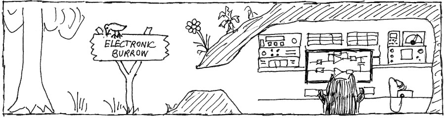
(An aside. I have had terrible trouble getting this Blog post to you. WordPress has fought me all the way. I still don’t know why so much user hostility has been programmed into it, but work-arounds have been found and here we are. I would like to acknowledge the help of the people from my site provider, Zuver. Thanks, Guys!)

On Tuesday the 23rd of July, I attended a seminar on LTspice. This was put on by the Arrow people. The speaker was Mike Engelhardt, the author/creator of LTspice. Mike is a proficient and entertaining speaker. We could tell that he was enjoying himself. Well he might, as it seems that he has a lot to crow about. He listed the respects in which he can claim that LTspice is superior to any other spice simulation package that is available to the public. The claims really are big. In taking in the Engelhardt story, we face a stark choice. We have to make one interpretation or the other – seems to me that there is no middle ground. The choice is this: Either we have to conclude that Mike really is laying it on a bit thick, or that LTspice is pretty special, and really is superior to other spice invocations – in spite of the fact that it is free. My bullshit detector did not go off, and I am inclined to the second view.

Mike Engelhardt in funny hat
(The hat wasn’t worn at the seminar)

I think that Mike finds an Australian audience a bit strange. He lists his achievements with this package, and these are achievements that anyone would be proud of, and the audience just sits there like stunned mullets. I get the impression that audiences in other places might be a little more demonstrative about being impressed. At one time, Mike said “Now I am going to step out of ‘Humble Mode’ ”. He then described some feature of the software that he is quite proud of. This was the second time that I had heard Mike speak, and I remembered that the first time ’round, I noted the way the Australian audience did not show appreciation. Thus when Mike made his brief statement whilst out of ‘Humble Mode’, I started the clapping off. Once it was started, the whole audience joined in. It was as if Australian audience members are a little embarrassed about showing that they are impressed, but once given permission, they let loose.

I remember the day, it would have been in 1989, that my colleague Tino Vescovi explained the significance of current mode control in a switched mode power supply to me. He explained that the supplies (topologies that we were looking at) had an inductor in series and a capacitor in shunt at the output. This is two poles in the control loop for voltage control. On the other hand, if we had current mode control, then the inductor was effectively being fed with a current. A current source in series with an inductor is just a current source. In other words the inductor disappears as far as the (outer) voltage control loop is concerned. This means that the loop has one less pole. There was more to it than that, in the Vescovi story, of course, but that was “Point Number One”. This is pretty fundamental in the world of switched mode supply design, and if you gathered a bunch of people who claimed to be switched mode power supply designers, then I would expect them all to know this: either that, or they had delusions of grandeur in claiming to be in the group.

On the first occasion that I heard Mike (2011), mates of mine who, like me, are switched mode power supply designers, Bob Sheehy and Nigel Machin were in the audience. When Mike asked what phase shift was caused by the inductor, one of us (I can’t remember which one), called out “None”. At the time, Mike said that he was impressed to find someone who knew that. Mike is a good speaker, and finding an excuse to flatter an audience member, is a ploy in his tool box of presentation tricks. On that ground, we can forgive him for making a fuss, but strictly, we should expect all of the audience to know this.

This time around, Mike again asked how much phase shift the inductor caused, and Bob and Nigel were not there, so it fell to me to call out “None”. Mike repeated his speil about how impressed he was to find someone who knew that. He obviously didn’t remember his first visit as well as I did. That didn’t matter. I went up a couple of hat sizes and enjoyed the rest of the seminar even more.

During the talk, Mike explained how we should draw conclusions about stability by identifying poles and zeros in the circuitry surrounding a switched mode controller chip. One pin on the chip was the output of a transconductance error amplifier. Attached to this was a capacitor and resistor in series to ground. His talk proceeded on the assumptions that the audience knew what the error amplifier was and its role in the scheme of things. These assumptions seems strangely incongruous with the assumption that the audience member did not realise that a current source in series with an inductor is just a current source.

I didn’t make notes to cover the whole substance of the talk, wanting only to record the information that was either new to me and I wanted to use, or, if not exactly new, then nice to be reminded of.

*** One was a method for investigating a system with feedback which requires the feedback for stable operation. There are many examples where we cannot just “open the loop”. A switched mode power supply would be an example. Another example is the Photo Diode Amplifier that I looked at in the posting to this blog More Photo Diode Amplifier – Investigating Miller Capacitance.

Mike’s method is to place the voltage generator that will introduce a disturbance in series with the feedback impedance.

*** Mike urged us to not use vendor’s spice models. He painted a word picture of a scenario in which a component manufacturer finds he is forced to provide spice models, and employs an intern to do the job. As presented to us, the story was entertaining. The horrible thing is that it could quite often be true!

*** If a circuit is complex and run-time might be an issue, don’t put capacitor esr in as a separate component, but put it in as an attribute of the capacitor. This reduces the number of nodes.

*** jfet op amps have a noisy tail current source, so need the same impedance on both inputs so that noise via source-gate capacitance will be (all) common mode. This is not a spice trick, but it is worthwhile point to remember.

*** One is usually better off not using initial conditions ( .ic ). Provide a circuit to add charge (to a capacitor, say) at the start of a run. Mike gave an example with a piecewise linear current source.

Placing one volt on a capacitor at the start of a run
without using the .ic statement.

 It is not clear to me why this is a curved line: I had expected a linear ramp.
(On reflection later, I realised that this had been a very clever way of steering us away from using the .ic command. I wonder what problems there are with the .ic command implementation in LTspice.)

A bunch of files relating to the seminar are to be found in this zip file:

http://ltspice.linear.com/LTspiceWorldTour.zip.

In a Readme, Mike has written:
The .zip archive usually doesn’t preserve the executeability of the .exe files contained therein. You will have to make them executable if you want to be able to use the links in the PowerPoint presentation like I did during the seminar.”

Still nothing worked for me, and after placing a query with John Simpson at Arrow, the following message came through:

It depends on the version of PowerPoint.  Often on has to
hardwire the absolute URL into the links.  The easiest way
to find the file is to right click on the link(in edit mode,
not presentation mode), note the name of the file, and then
open that file.  The file will be in the .zip file.”

I can’t really understand this. I can open the Power Point file in Power Point or in Open Office, but cannot work the hyperlinks off the slides. I don’t regard this as an LTspice matter. I have never before taken any interest in Power Point, being content to just use it as a slideshow viewer, and now I suppose I pay the price.

Another Way?
Apart from attending excellent seminars featuring Mike Engelhardt, there appears to be another way to learn more about LTspice. This is by purchasing a heavy hard cover book that is published by Wurth Elektronik who are another Linear Technology dealer. Wurth Elektronik are a German company. They have several factories, and I could not identify a “Head Office” location on their website, so I can’t say where they are from. I bought my copy from the local Wurth Elektronik office, or perhaps I should say I “picked up” my copy from the local office, as the transaction turned out to be an international transaction in US dollars with an office in Singapore.

It is immediately obvious that the book was not originally written in English. Indeed it is obvious that the translator is not familiar with English idiom. Many a turn of phrase makes strange reading until you realise that some probably popular and common expression in German has been translated word for word into English. The writing style reminds me of the writing style that is prevalent in Elektor magazine.

Quite apart from our languages being different, I think such things as conventions about how material should be laid out for a reader’s convenience are very different. I have enjoyed reading the book: it is a bit like reading Finnegans Wake (sic): you read the actual words, and then you think a bit about what the words mean. I found a couple of what seemed to be errors, but then again, perhaps I was not converting the words into my own vernacular correctly! It is easy to understand how these difficulties arise. Just imagine the distinction that we make between the words “valuable” and “invaluable”. If I employed a youngster to translate my words into German and then where I wrote “invaluable” a German reader read the German equivalent of “not valuable”, then she might reckon that I had made an error.

I had two particular questions about LTspice that had arisen when actually working with it. The first was that I wanted to know how to make an assignment statement. I had been using stepping in spice for some time:

.step param R 1 10 3

(that sort of thing)

but when I am exploring a multidimensional concept space, I might want to step through one parameter at a time whilst keeping all the others constant. My idea was that I could step on R (as above) whilst assigning values to R2, R3 and R4 (say), and then later step on R2 and assign a fixed value to R.

After a quick and casual (no written method) attempt to find out how to do this in the Wurth book, I wrote down all the words that I could think of that were synonyms of “assignment statement”. I probably have to admit here that my imagination wasn’t very good. I then searched the index. None of them were there.

My second question was to do with the FFT plot. Could I show this with a linear frequency scale?

The index of the book has four entries for “FFT” (pages 43, 36, 36, and 76). Page 36 has nothing about FFT except that we should look at Chapter 8.
Page 43 has nothing about FFT, but the text string “FFT” does appear in a list of file types that LTspice works with.
Page 76 contains instructions for a parrot to repeat some steps which lead to an FFT to appear on the screen. This is fine as long as the parrot doesn’t want to know what it is all about.
Chapter 8 starts on page 170 (a page not mentioned under “FFT” in the index) and is headed:
MEASUREMENTS, VIRTUAL OSCILLOSCOPE AND FFT EDITORS”

At first, one might not worry just what this chapter title means. Notice that the word “editor” is in the plural. I didn’t worry about this when I first encountered it, but later I came to believe that I had been informed that there are three editors:

(i) Measurements Editor
(ii) Virtual Oscilloscope Editor
(iii) FFT Editor

When reading the chapter, I encountered a sub heading:
8.3.1 Virtual oscilloscope and FFT analyser editor”

Does the singular form of the noun here tell us that one editor serves both?

Then again, what does “Editor” mean? This seems pretty unambiguous, but I remember when I first encountered the word “Editor” in a computer context. It would have been about 1978, and I had just purchased my first Editor and Assembler (both came as punched paper tape, and ran on a Motorola 6800 system). I had great difficulty getting these going, not because of any technical problem, but because of a semantic one. In my mind, editing meant changing some written material. This meant that before you could edit something, you had to write it. In the days when the text i/o was by way of a teletype, editing was a tricky business. You had to print out the document and then identify the place for a change by line number, and then type in a replacement or additional line to go in that spot. A cumbersome business. I could understand that as programs that would fit on a punch paper tape went, this was tricky and I would need a program for that. But how the hell do I enter my text document in the first place? Then I discovered that in the world of the computer, editing does not mean editing! No, it means writing AND editing. This would all be so obvious to young people that the story must seem strange. It is just the way the language goes. What was the German author thinking of when he wrote the German word that was later translated as “Editor”? We don’t know. Could it have been ‘Pop-Down Menu”?

The reason for this musing, is that I have read Chapter 8 very carefully, and cannot find any evidence of an FFT Editor apart form the heading quoted above!

On the day of the seminar, whilst school was out for play time, I collared Mike Engelhardt and asked him my two questions. these were answered in less than a minute.

So far the Wurth Elektronik book has cost me more in time than in purchase price, and I haven’t learned anything from it yet. In spite of this, I do not regret owning it. The fact that it exists probably reduces the probability that someone else will write a book on just this topic. Thus it is the ONLY book on this. That probably makes it a bit special, even if nothing else does.

The answers to my questions were:
(i) The assignment statement in spice is “.param” as in “.param R=5k”
(This IS in the Wurth Elektronik book: one just had to know which word to search on.)

(ii) If you move the cursor towards the bottom of the FFT plot, at some point it will turn into a little ruler. Click and a pop up menu will offer you some options. One of these is a box with a tick in it labelled “Logarithmic”. Remove the tick with a click. This is not exclusive to the FFT plot.

There is a third way to obtain information about LTspice. The program is very popular, and there are many tutorials and even videos to help that are only a Google search away.

Then there are the help screen in the program. I gather from my Googling that these have a bad reputation. They were mentioned several times by Mike in the seminar, but always in the context of the one statement:

I would not be so condescending as to suggest that a person look at the Help screens”. If you can figure out what that means, you should have no trouble with the Wurth Elektronik book.