Dear reader,
If you were interested in my first posting on negative Resistance, then I must apologize for such a long delay before I return to the subject. Pressure of other things.
In the first posting, I resorted to an old trick of offering a packet of Smarties as a prize for the best answer to a question that had been put to the readers of Wireless World in April in 1939. I suppose that date puts things in perspective and makes my delay of a few weeks in returning to this look pretty minor.
You might be wondering where this Smarties business comes from, and what place it has in this serious blog. It all started when I was to address an Historical Society on historical railway matters. I was warned that I might have trouble holding the audience attention. Thus alerted, I planned out several tricks to stimulate audience involvement. Of these, the handing out of little packets of Smarties as prizes for correct answers to questions proved to be the most effective. It is amazing how competitive a room full of senior citizens can be!
So, having brought the joke into this forum, it falls to me to “pay up”. Packets of Smarties have been sent to Brian Magee and James Fenech.
I had gone into this a bit right after the first posting on the matter, and now I come back to my notes, I find that this process seems to be an interesting bit of industrial archaeology in itself. To model what was going on in the Wireless World Circuit (See my earlier posting “http://richardschurmann.com.au/Other/Electronic_Burrow/?p=335”), I chose to use a cubic to provide me with an anode characteristic that had the essential features of the tetrode described. I scratched around with some algebra to work out the equation for a cubic that would seem to pass through the key points. I ended up with:
I = 0.000134 * (0.678E-3 * v^3 – 0.884E-1 * v^2 + 2.9 * v)
The non canonical form of this is a product of the way I derived it. I did not attempt to simplify the presentation of the polynomial, as I could rely on the simulator to multiply out my coefficients at run time.
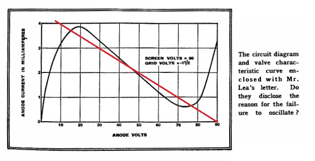
Here is the tetrode circuit and characteristic as published all those years ago. I have added the load line for the 20k dropper resistor.

Here is the result of the simulation:
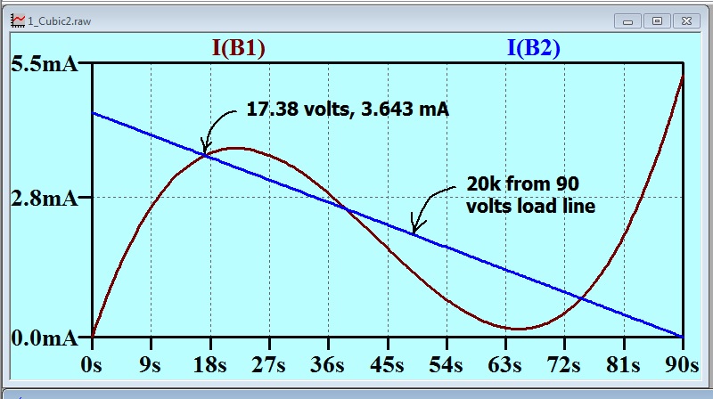
Not the same, but near enough to explore the key points.
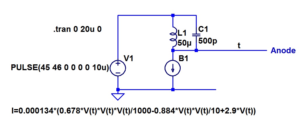
Here is the simulation circuit:

Notice that I have set up my “curve tracer” by offering the cubic response generator with a voltage ramp, which I created by providing a constant current to capacitor C1. This is scaled so that the voltage rises one volt every second. This means that a time domain plot with a time scale marked out in seconds can be read as if the horizontal scale is a voltage scale. The current B1 is the tetrode anode current, and current B2 is for drawing the load line.
The above simulation just showed how my arbitrary function generator loaded with a cubic represented the key features of the tetrode plate characteristic. Then I put that tetrode in the circuit.

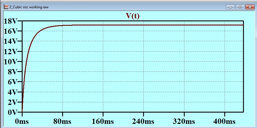
You can see that the voltage rises to the first crossing point of the anode characteristic and the load line (round about 17.38 volts).
On the other hand, if we power the anode circuit from a low impedance supply at 45 volts, we might get the successful oscillator circuit that was originally wanted.
If we run this, we get the Anode Voltage coming out like this:
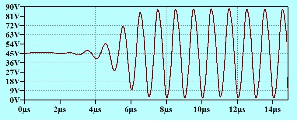
Which is what was wanted in the first place.
More on this in another post later.