Category Archives: Uncategorized

Current Source 3

This is a minor posting to follow up a point raised in response to one of the previous Current Source posts. Several people sent me emails of the form “Why don’t you….?”. In Current Source 2, I explained that the application was for building by ‘hobby people’ with a production run of 1 (each). This makes any specialized current source ICs unsuitable. James Fenech asked “Why don’t you use an op-amp?” James knew perfectly well that I had used an op-amp for a very similar task on a previous design. Below I show (with permission of the intellectual property owner) a circuit which used a quad op-amp to provide pulse width modulation. This was designed by me, but is not drawn as I would draw it. I have taken this diagram from a much larger and complex one, and this circuitry had to fit on the page amongst other things. In this case, there is not a module of circuitry that one would identify as “the current source”, which plays the equivalent role to the current source in the last post, as it is a single resistor: R14. Unfortunately, you might not be able to identify R14 on the circuit diagram (This is a problem with this blog software – not enough resolution for diagrams! If you wish, you can view a higher resolution copy of this here: .pdf of op-amp based circuit ) It is the resistor feeding current to the inverting input of the op-amp labelled “Integrator”.

Composite

In this particular application, the requirement was to sense temperature across an isolation barrier. An opto isolator was already in the design to pass a pulse stream for other purposes, so this circuit was added to hitch a free ride on those pulses by modulating their width. I won’t attempt to explain every detail of the circuit operation, as you can figure it out for yourself, although there is a trap in there for the unwary.

Note that the amplified voltage from the temperature sensor is “mixed” with a bit of DC from the regulated supply (the resistor immediately above the Integrator) We didn’t want the pulse width to diminish to zero as the temperature fell to zero.

The “Trap”? I designed this circuit, and got it working, without understanding it fully (even though I had several pages of notes to support the design). What I hadn’t allowed for is that in the time immediately before the integration ramp, the Trigger output is high and the Integrator output is saturated low. The integrator capacitor will thus charge up (plus at the left end as shown). When the trigger changes state, the capacitor will have to discharge before the integration ramp can start (the integration ramp involves charging the capacitor with the right end positive). I designed this, and missed this point. The circuit was inspected by several very clever engineers and they missed this point as well (So I don’t feel so bad). This delay to the integration ramp did not matter in the application, but I did not want any of that sort of second order complexity in the circuit at the end of the previous post (Current Source 2). So James, that is why I did not use an op-amp in Current Source 2.

Current Source 2

Towards a Temperature Compensated Current Source.
Second Post on Topic

17-05-2013

Synopsis.
I continue to look at current sources for an application in which the temperature coefficient had to be kept under control. This post assumes that the reader has read my previous post on this subject. If you have not read that, seek it out before reading this.

Requirement
The application is a pulse width modulator in which a fixed current is applied to a capacitor to provide a “time – voltage” relationship. The application does not require very high accuracy or linearity, but a couple of set points on the range (min and max) have to stay pretty well where they are put. (Just exactly what “pretty well” means is not determined yet.)

There are two ways from here
The narrative splits into two at this point. I will have to deal with them sequentially. When you get to the second branch, just remember that this is where it branches off.

Current Source Thread Branch 1.
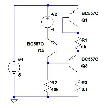
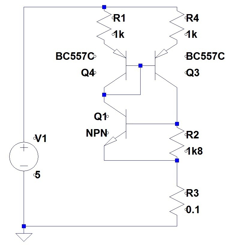
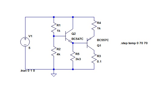
Just a reminder, this is the current source circuit that I had at the very end of my last posting.

CS2-1

On simulation, this yields output current from 0.99954mA to 1.00026mA over temperature: a change of 720nA. (The temperature range I had selected for these tests was 0 degrees C to 70 degrees C) The actual sequence that lead to this circuit was not exactly as I had stated in the last posting. I had been tweaking the values of the resistors R5 and R2 and found that my optimum was at almost identical values before the reason that they would be almost identical became clear.

By the time I was writing out the last posting, it was obvious why:
(a) They are almost identical
(b) Choosing the same value in “real hardware” would be near enough
(c) The optimum values I had found by iteration in the simulation were not exactly the same.

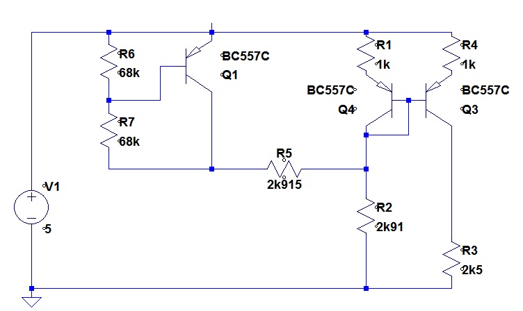
Just to clarify in my own mind exactly how the temperature compensator was influencing the mirror, I went into the matter in a little more detail. Some of you will be way ahead of me, but others might find this clarifying.

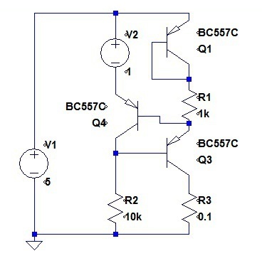
Here again is the raw current mirror.

CS2-2

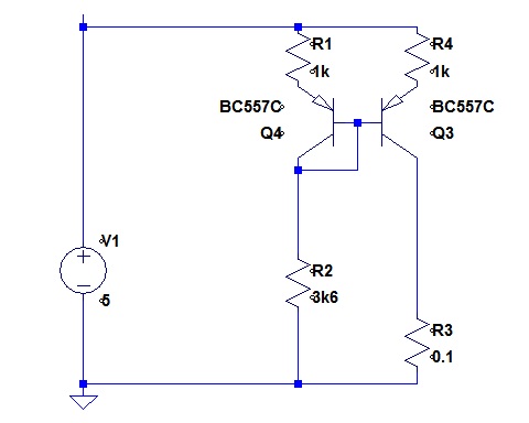
Remember that I had identified that the main temperature error (assuming identical transistors) arose because the current in the left branch has to traverse:
(a) R1
(b) VBE of Q4
(c) R2

As the VBE of Q4 varies with temperature, the volt drop left to share between R1 and R2 changes, and thus the current changes. The temperature compensator replaces R2 as a current sink for the Q4 collector.

CS2-3

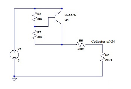
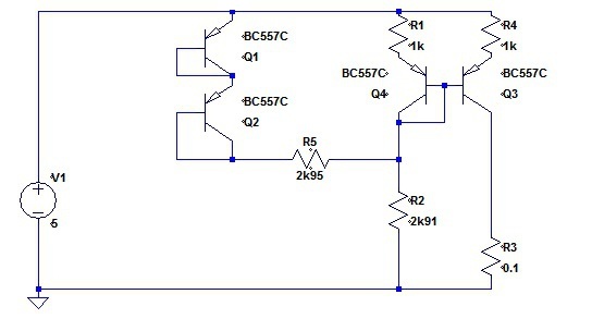
I like to show voltage dividers as voltage dividers, and a change to this yields:

CS2-4

Replacing the VBE multiplier with a voltage source symbol changes the circuit to:

CS2-5

The voltage source V4 has a magnitude of output of two times VBE. Notice that I called this 2 x Vj (for Voltage of junction) as the circuit capture on the low price spice does not provide for subscripts.

It should be noted here, that there is nothing, as far as I can see, that is magical about the number 2. This circuit would work if V4 gave 1.8 times the junction voltage and then the voltage divider divided by 1.8. Indeed, there might be some reason for choosing a number other than 2, but I am not going to pursue it in this posting (see below).

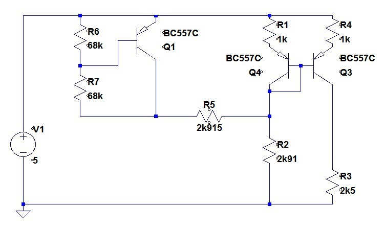
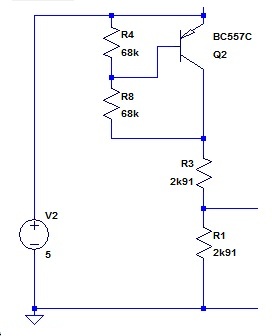
When we encapsulate the voltage divider in our model, we get:

CS2-6

The voltage source is halved, and the output resistance is the resistance of the two divider resistors in parallel. Now let us reunite the temperature compensator with the left leg of the mirror.

CS2-7
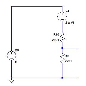
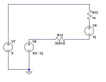
There are three voltage sources in series around this loop. Lets incorporate them all into one.

CS2-8

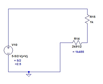
The voltage across the resistors has no contribution from any junctions within the limits of all the assumptions, stated and implied.

My third obvious point above, (c), was that it seemed obvious to me why I had found an optimum in which R5 and R2 were not exactly the same. I reckon that it is because the junction that has its volt drop multiplied in the VBE multiplier is not carrying the same current as the junctions in the mirror. I have observed that we can multiply, and then divide this VBE by some number other than 2. I reckon that in this way we could change the current in Q1 so that it matched that in the mirror transistors. Some tricky maths might yield a simple answer that would give us different resistor values and a better optimum. I am not going to go there now for two reasons. First the optimum is pretty good already, and second, this is the place to terminate this branch and go back up to the branching point and look at the other.

Current Source Thread Branch 2.
After I had posted the last posting on this, I was looking a bit further on the web and I had one of those “D’oh!” moments. (Is that how you spell it?)

CS2-9

I found a circuit that was simpler than the one I have developed above and which will most likely be good enough. It reduced the transistor count from 3 to 2. I do not remember ever seeing it before, but that is no excuse. As soon as I saw it, I could see that it was so obvious, that not thinking of it was inexcusable. I will record that I had several replies to the last posting, and one of them was on to this (after I had found it). The circuit was in a group of images that Google offered me when I Googled “Temperature Compensated Current source”. I tracked it down to:
http://www.radio-electronics.com/info/circuits/transistor/active-constant-current-source.php
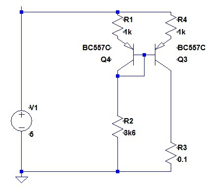
… a site I do not particularly recommend, as it is written at too simple a level for readers of this post. Their circuit was:

CS2-10

As I wanted a current source and not a current sink, I took the simple step of turning it upside down.

CS2-11The operation is obvious: (to a first approximation) the constant voltage determined by the divider R1 and R2 has one VBE subtracted from it, and then a VBE added back to it. The two VBEs can be contrived to match reasonably well if the two transistors carry the same current.

This arrangement was adopted in my circuit. I had described the requirement earlier, but I should perhaps add that this circuit is for publication in a hobby magazine, and might go on to be constructed by a number of amateur constructors. The optimum economy in the design will thus be different from most design projects. In particular, the product cost is the BOM cost. Labour is costed at zero. Secondly, component availability is an issue. One lot of freight cost from Digikey will buy a lot of parts from Altronics or Jaycar when the purchasing is being done for a production run of one. This is why I have not chosen one of the monolithic current sources.

Here is my back-of-the-envelope sketch of the module incorporating the current source (as drawn before I went off on this “minimizing tempco” quest).

CS2-12
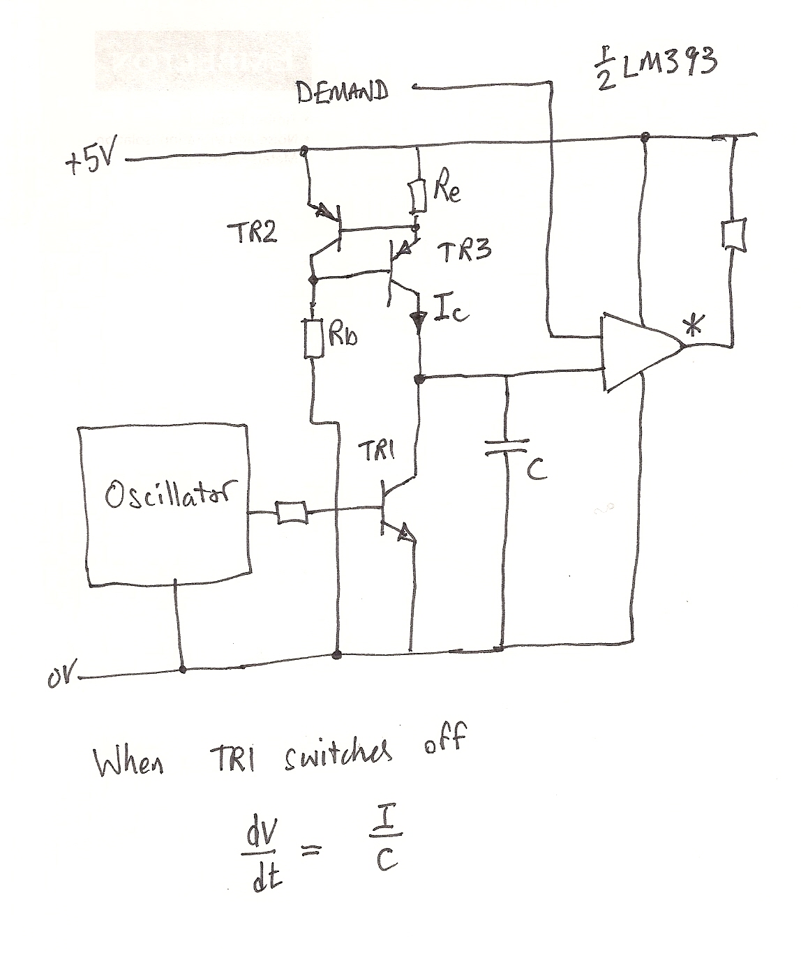
In this application, a “servo” of the type that is used in model aeroplanes and the like is used to activate an engine throttle. The reason that I had written earlier that “couple of set points on the range (min and max) have to stay pretty well where they are put” was that these are the stops in the throttle linkage travel. I place “servo” in inverted commas as in this context the word has come to have a quite different meaning from that used elsewhere. These little jiggers take as input a pulse train, and adjust their position according to the width of the pulses. The requirement to drive one, then, is a repetitive variable pulse width. Here is the circuit a little further down the development track.

CS2-13

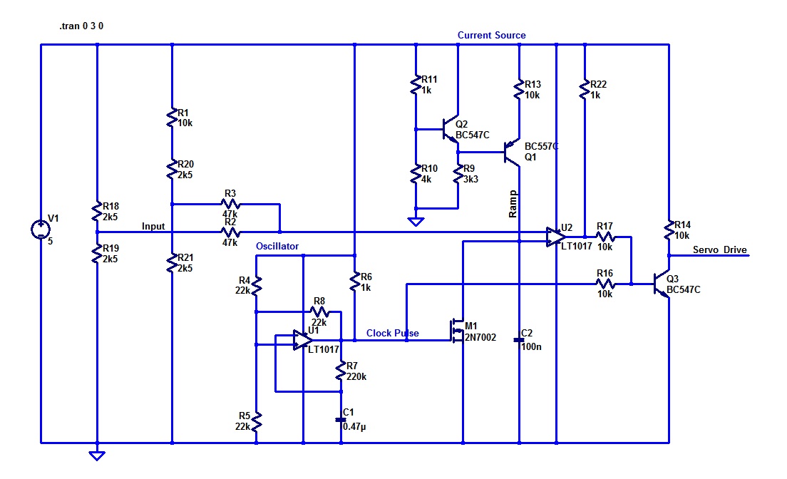
For reasons that are logical, but which I will not go into here, this circuit has some anomalous resistor values showing. If the dual comparator is changed from a LT1017 to an LM393, and the MOSFET changed to a 2N7000 (both changes will have no impact on operation) then the requirements about component availability are met. I only have two line thickness for the reproduction of the circuit above, and I have chosen “thick”. This makes the comparator symbols very unclear. To help you read the circuit: the inverting input is at the top and the non-inverting below it.

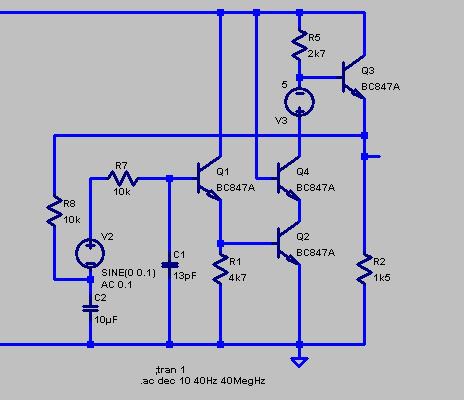
Here (in simulation) is the “Servo Drive” and the “Ramp” signal.

CS2-14

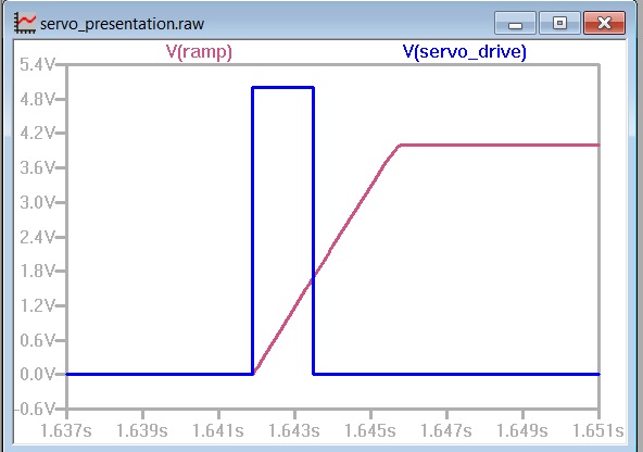
The timing of the falling edge of the output pulse (blue) is determined by the voltage on the ramp.

R.

Current Source 1

Towards a Temperature Compensated Current Source.
 08-05-2013

In the text below, I use the term “transdiode”. If you have not encountered this term before, you will, I am sure, find the meaning obvious. This is not a matter of me making up words or picking up new trendy ones. I picked up the term from Peter Baxandall and Douglas Self.

Synopsis.
I had recommended a cheap current source circuit to a colleague. On reflection, I was concerned that the temperature coefficient might have been too high. I explored several alternative arrangements and found that the temperature coefficient could be vastly improved. I have restricted this to circuits with small number of transistors and resistors. Circuit modelling has been done with LTSpice. This provides for variations in temperature, but I do not believe it is correcting for variations in rise above ambient for different silicon chips according to their individual dissipations. The optimum that would be obtained with real hardware could not be expected to be as good as I have obtained in the simulation.

Requirement
The application is a pulse width modulator in which a fixed current is applied to a capacitor to provide a “time – voltage” relationship. The application does not require very high accuracy or linearity, but a couple of set points on the range (min and max) have to stay pretty well where they are put. (Just exactly what “pretty well” means is not determined yet.)

A crack at it
My starting point was a circuit that I have always known as the “D2 current source” as I have associated it with a colleague whose nick name was “D2”. I do know that he didn’t invent it, and maybe it has a proper name.

I record here several steps I took whilst I explored the options for reducing the temperature coefficient of the current source for this application. I chose a design current of 1 mA. there is nothing special about this figure, and indeed, there might prove to be good reasons for diverging widely from this. I believe that what I have discovered here would apply just as well (with appropriate adjustments) for other quiescent conditions. As I tried different circuits, I did not attempt to adjust the output current: not, that is until just near the end. CS1-1

This is the basic D2 Current source with resistor values chosen to give a nominal 1 mA output. The resistor R3 is in the circuit for the simulator (LTSpice) to have a component to measure the current in. Over the temperature range (0 degrees C to 70 degrees C), this yields 720uA to 920uA a Delta of 200uA. That is a fifth of the span. Not good enough for the application. In this circuit, the output current is determined by the comparison of VBE for Q4 and the volt drop in R1 carrying the output current. First order base current cancellation takes place, as the base current of Q3 is added to the output current on its way to R1, but then the base current of Q4 is subtracted. One idea is to correct for the VBE drop of Q4 and then add a more stable volt drop. One of the band gap devices might serve. This gives the following circuit.

CS1-2

V2 represents a “perfect” one volt band gap device. This now provides the volt drop to compare the volt drop in R1 with. The transdiode Q1 cancels out (to an extent) the temperature sensitive VBE of Q4. This gave a range of 788uA to 830uA over temperature, a delta of 42 uA. This is better.

It occurred to me that the above circuit was using the transdiode Q1 which is carrying pretty well the output current to cancel the VBE of Q4 which is carrying very much less current. One trick might be to increase the current in Q4 to a value much the same as the output current.

CS1-3 This is easily achieved by reducing the value of R2. I chose 2k8. the result is an output current of 0.9995mA to 1.0011mA over temperature, a delta of 1.6uA.

This is pretty good. (Much better than is needed for the application) but it does involve the use of that perfect 1 volt band gap device. can we do without that? What about a current mirror?

CS1-4
This gives an output current of 884uA to 913uA over temperature, a delta of 29uA. Better than the plain vanilla D2, but maybe we can do better yet. I thought of a two terminal current source circuit that I devised many years ago for a completely different application.

CS1-5

This gives 770uA to 890uA over temp, a delta of 120uA. Not promising. I went back to that current mirror to see what I could do with that.

CS1-6

The trouble with it is, I reasoned, that the five volts is divided up between:
1. The volt drop across R1
2. The volt drop of the transdiode Q4
3. The volt drop across R2.

Of course, item 2. varies with temperature, which imposes a variation on the other two. The variation in item 1. translates directly into variation in output current. What can we do to keep the current in R1 constant? One trick would be to vary the voltage at the collector of Q4 with temperature. If instead of just having R2 there, we had some circuit that varied the voltage on the collector of Q4 by just as much as the forward volt drop of Q4 configured as a transdiode would vary.

One way to do this, is to start with a supply voltage that varies twice as much as Q4 does, and then divide this variation in two with a resistive divider. If the current flowing from Q4 upsets the perfect division by two of the voltage divider, then maybe we can compensate by tweaking the dividing ratio a little. Here is the result.

CS1-7 The collector of Q2 will be at a voltage that is two transdiode drops below the five volt rail. R5 and R2 divide this voltage by a factor that is slightly off one half. In my reasoning for the divide ratio (above), I allowed for variation from the the exact factor of one half. I imagine that other factors come into play as well. Q1 and Q2 will not be carrying the same current as Q4 for a start. The values of R5 and R2 sown here are only 1.3% apart.

In this case, as I was coming near to the end of my quest for a cost effective low tempco current source, I did go to the trouble to tweak the resistor values to get closer to the design current specification that I set myself.

The result is: output current varies from 1.00028mA to 1.00029mA a change of 10nA!
(Please forgive the exclamation mark. I am pleased with this result.)

What if we make R5 and R2 the same value (a practical thing to do)? I will choose 2k91, an E96 value. The output current degrades to variation between 998.88uA and 999.23uA, a variation of 350nA. This does look a lot worse than 10nA, but I suspect that this difference would not be significant with real world components.

The emitter resistor should have tight control of the current in Q3, so I do not expect much Early effect influence.
Output current with R3 = 0.1 ohm (default temperature) = 1.000215 mA
Output current with R3 = 2k5 3k (default temperature) = 997.407uA

Effective output impedance = delta V/delta I
= 2.5/2.8E-6
= 890k
I thought it would be higher than that.
A variation in 2.8uA in a 1 mA current as a connected capacitor is charged will not be a problem in the application.

An afterthought.
I just thought “VBE multiplier” and saved a transistor. No efforts to optimize this at this stage.

CS1-8

More Photo Diode Amplifier

More Photo Diode Amplifier – Investigating Miller Capacitance

In response to my posting of 31st December, my mate Nigel Machin left a comment that he thought that the miller capacitance of the voltage gain stage (Q2 in the CA3127 implementation, and Q11 in the discrete transistor version) would provide the dominant pole. The whole idea of this circuit was to have no pole dominant over that provided by the photo diode capacitance. The CA3127 transistors have hFE of 1 GHz, whereas my BC847s are a lot slower, and in simulation (but not in the hardware of the product) there was a little peak, indicating conjugation of closed loop poles.

I wanted to investigate this just a little further. Here are two moves I made in the LTSpice environment to understand this circuit a little better.

First, I wanted to open the loop. This circuit relies on a closed loop for DC conditions, so we need a loop that is closed at low frequencies and open in the frequency range of interest (where the diode capacitance and the the miller capacitance are introducing poles).

So here is the first move.

Image 1

The voltage generator V5 will be where I will introduce the AC signal for the Bode plot. The minus end of this is where the low frequency feedback is introduced. The feedback will reduce the gain, but when you see the Bode plot later you will see that the low frequency fall off in gain is decades away from the frequencies of interest. R10 will represent the loading that is applied to the emitter of the emitter follower in the real circuit. The emitter of the emitter follower is where I have opened the loop for high frequency considerations. R9 represents the feedback resistor in the real circuit, in its role as part of the loop. C3 is the capacitance of the photo diode.

Now this circuit gives me a path around the feedback loop but with the loop open, starting from the signal fed to the feedback resistor (Left end of R9) and then through the forward path to the emitter of the emitter follower output stage.

The second move is to do the same thing again, but to make a huge reduction in the Miller capacitance. I have done this by replacing the voltage gain stage (Q6 above) by a cascode.

2

I have chosen the 5 volt rail as a suitable point to tie the base of the top cascode transistor. This means that, allowing for some voltage swing, I need the collector of the top cascode transistor to be at a voltage that is somewhat higher then 5 volts. Fortunately, in the model world, we can pull stunts that would be tricky with real hardware, and I have raised the voltage of that collector with the fully floating voltage generator V3. The minus end of this will be at about 4.4 volts, so the plus end, the cascode transistor collector, will be at about 9.4. That will do nicely.

Now instead of having a voltage gain of about -100, Q2 will have a voltage gain round about -1.

This will reduce the impact of the Miller capacitance on the base of Q2 by a factor of 2/101. I built both of these circuits in a single model, which is just a simpleton’s way of providing for both Bode plots on the same axes.

Revised image (624 x 279)

Here are the Bode plots

4

The colours are:

Dark Green – Open Loop gain of cascode Circuit (emitter of Q3)

Light Green – Open Loop gain of original circuit (emitter of Q7)

Red – Voltage at photo diode (C1) in cascode circuit

Blue – Voltage at photo diode (C3) in original circuit.


Notice that where the Blue line is lower than the Red line, this means that the Miller capacitance is lowering the impedance at the diode (and this effect is greater without the cascode), even though there is that input emitter follower in between.

The time constant in the open loop path that is presented by the feedback resistor and the photo diode capacitance is 130 ns, which corresponds to ω = 7.7E6, and f = 1.22 MHz. (this is ignoring the impedance presented by the base of the first stage, which we know has some capacitive component.)

It is interesting that the phase margin for both circuits is about the same – 20 degrees, although the Cascode has unity gain at a little over 6 mHz, and the original circuit has unity gain at a little over 3MHz.

Transistor Photo Diode Amplifier

Transistor photo diode amplifier

In my first posting “ADALPAD”, I showed an example of an op-amp used as a photo diode amplifier and with a trimmer across the feedback resistor. That circuit (a nightmare from my past) had come to mind when I explored an idea I picked up in ADALPAD.

In some applications where fast transitions have to be reproduced, it is common to use a transresistance amplifier with a photo diode. This ensures a very low voltage excursion at the photo diode and thus very little charge wasted charging and discharging the diode capacitance. The diode capacitance together with the resistance driving it, creates a pole in the feedback loop. Instead of designing a two pole system with the diode capacitance and the op-amp dominant compensation pole, it is easier to leave out the op amp pole and let the diode capacitance provide a dominant pole.

Here is a circuit from Application Note 915 of the 1983 HP Optoelectronics Designer’s Catalog (sic) 1983. “Threshold Detection of Visible and Infrared Radiation with PIN Photodiodes”

(pp503 Figure 8 High Speed, High Gain Photodiode Amplifier)


transistor photo diode amplifier


The CA3127 is a monolithic array of uncommitted transistors.
These have hFE(min) = 35, and fT(min) = 1 GHz. I used this as a basis for several designs of my own. I did not need that bandwidth and was able to use discrete general purpose transistors. (See below for thermal issues) I was also able to increase R1 to get all the linear amplification I needed in the first stage. One application was data which was transferred at 9600 bits per second. At this data rate, it was vital that the linear amplifier was restricted to its linear range. Any saturation or cut-off of Q2 led to a failure of the feedback and a change in the charge on the diode capacitance. This in turn disabled the circuit which then took too long to recover.

One application, an optical communications port on a kilowatt hour meter, required operation over a dynamic range of more then 10:1. This could be easily allowed for by choosing R1 so that with the strongest signal, the output did not quite reach the maximum voltage of the linear range.

The elimination of R4 changed the second part into a comparator which provided a logic output. On some variants, I eliminated the emitter follower altogether.

The second stage of this circuit has an interesting and subtle feature. It is really a differential comparator (comparator below, differential amplifier above) , yet the usual differential input feature, the long tailed pair, is missing. The differential comparator, to act as a differential comparator, has to compare the voltage on the base of Q4 with what the voltage on Q4 would be if the circuit was in the quiescent state (no light on diode).. This is clearly two VBE drops (base – emitter junction of Q4 and Q5). The circuit cleverly provides an offset of just two base emitter junctions, as this is the output voltage of the first stage when there is no diode current, if we can ignore the volt drop in R1 due to Q1 base current.

Below is a schematic snippet of one of my implementations of this circuit.


My application


I do not still have the design notes for this, but the schematic brings some of the story to mind.

At this stage in the development of the thinking about the circuit, the emitter follower was still hanging in there, but I suspect it was not justified. The diode D26 is labelled “VESCOVI CLAMP” in the formal documentation. Of course it is a Baker clamp, but the special name is to honour my mate Tino Vescovi who realised the reason for a problem I was having. If the transistor Q20 had a high hFE, then the emitter current could be excessive in strong signal conditions. This warmed Q20 and Q21 and upset the balance with the b-e drops of Q10 and Q11. The Vescovi clamp fixed this. OPTORECH did not thus pull down to a single VCE(sat), but was nevertheless a suitable logic signal for the selected CMOS logic to follow.

Note the 1M resistor R164 which provided about 80 mV hysteresis at the emitter of Q19. the voltage divider R116 and R160 was not present in the original circuit. This determined the photodiode current for the logic threshold.

A lot of tricks in there. I really only wanted to share this for the use of the photodiode capacitance for the dominant pole for the transresistance stage.


ADALPAD 2

In the last post I mentioned that we are so used to “Op Amp” thinking these days that we take some big simplifications for granted. An example is the output resistance of the op amp being very low. This resistance will usually break with stray capacitance at some frequency way out where we don’t care. In an example I looked at last time, we had a single stage exhibiting a two pole response. Of course the single stage (a BJT, say) will exhibit an output resistance that is not much lower than the collector load. It might break with stray capacitance at a frequency not too far removed from the frequency at which the input capacitance is having its impact.

Further on in ADALPAD, (pp 780 in Chapter 14 “Amplifiers with Multistage Feedback”) there is a two stage amplifier.

Two stage circ

 This circuit, or one very much like it, was promoted in “Radio and Hobbies” magazine when I was a high school student. I remember wondering at the time why two different transistor types were specified, when the duty seemed to be within the capabilities of either type. Looking back after all these years I would have to say that I suspect that the Radio and Hobbies people would not have known the answer.

The caption to the circuit in ADALPAD reads:

Fig. 14.35 Circuit diagram for an audio-frequency current -feedback pair. The gain is about 75, and the bandwidth about 8 Hz to 200kHz. OC44: alloyed germanium transistor, ΒN =60, fT = 10 MHz; OC71: alloyed germanium transistor, ΒN = 40, fT = 500 kHz.

Further down, the authors write:

Two stage text

 It all makes sense now. Note that as the feedback is taken from the second transistor emitter, the collector is not in the feedback loop, so stray capacitance on the collector will have little impact on the feedback loop. It is interesting that in those days a designer could choose transistors with confidence that their fvalues could be in a known relationship. Maybe in those days the transistor manufacturers had a lot of trouble getting a specified   fTand were selecting transistors for a specific “fT bin”. I don’t think that we could do that these days. My impression has been that transistor manufacturers generally specify a minimum value for fT and no maximum. I did a quick Google search on available data sheets and made up this table.

 What the data sheets tell us about fT

Table_cropped

My quick Google search yielded only one transistor for which a maximum as well as a minimum for fwas specified, and they are an octave apart. I have a very old transistor data book which I keep because it provides much more data about transistors than is generally available these days. (National Semiconductor Transistors 1973) That book does specify some transistors where both a minimum and a maximum value for fis cited. Note that the min and max are at least 2 octaves apart. This data does not provide for precise placement of poles in the transfer function of an amplifier design.

Come to think of it, have you ever seen a Maximum as well as a Minimum for the gain Bandwidth product on an Op Amp data sheet?

I think that circuits of the type depicted above are just not possible with today’s parts. One would have to place a capacitor somewhere to get one of those poles way below the other. 

In November, I attended the annual “Student Projects Showcase” of the faculty of Science and Engineering at LaTrobe University. This is the department that was set up by the Hooper of ADALPAD. In the program for the evening, there was a little spiel about Daryl Hooper and I was pleased to see that mention was made of ADALPAD. I wonder how many of the 2012 students had read it.


Hooper blurb


ADALPAD

A1-1

 ADALPAD

I first heard of the book Amplifying Devices and Low Pass Amplifier Design (commonly known as ADALPAD) after it was already out of print. The title seems a little strange as all amplifiers must have a finite bandwidth, so maybe they are all Low Pass Amplifiers. Perhaps the distinction is being made from tuned amplifiers as used in radio receivers (and transmitters). The book was written by Ed Cherry and Daryl Hooper, both interesting blokes. It was published in 1968 when vacuum tubes and germanium transistors were both still taken seriously. Many things have changed since then, but the principles have not. If there is a more modern book covering the same scope, I don’t know about it.

The monolithic operational amplifier now dominates the field, and this forces an engineer to take a different approach. Let us not forget how things work, even if things are so often made easy for us these days.

When I fist saw the book, I could not buy one, so I borrowed one and photocopied the whole thing. This is breech of copyright but Ed Cherry signed my photocopy for me, so he could have not been too resentful about missing out on his commission. The photocopy book was a little inconvenient, and since I copied it, the internet has provided easy access to the entire world second-hand book market, so I decided to treat myself with a real one. Mine is from the library of the University of Sunderland in the UK. This is not the first second-hand book that I have purchased that has come from a university library. My John Maynard Smith sex book
http://en.wikipedia.org/wiki/John_Maynard_Smith is also from a uni library. What are these librarians doing? What will the young kiddies do when they need to refer to these books and find they have been sold to me?

Oh Dear!

Years ago, I had located another out-of-print book Network Analysis and Feedback Amplifier Design by Hendrik Bode and had made myself a photocopy of that as well. I mentioned to Ed Cherry that I was struggling with it and he told me that he reckoned that he had made a rather good job of an exegesis of that in Chapter 14 of ADALPAD.

Last weekend was a long weekend away for us, so I took my new (to me) ADALPAD, and read Chapter 14 twice. That sent me off to read other chapters (prerequisites). I have been having a beaut time with it.

Chapter 13 is headed “Peaking”. In amplifier design, this is the creation of a peak in the amplifier response where there would otherwise be a hole or a falling away. I was flicking through, and found a capacitor across the feedback resistor in a shunt feedback stage.

A1-2

 My first reaction was that the capacitor across the shunt feedback resistor would introduce a pole to the closed loop response and lower the bandwidth. Then I realized that I had been guilty of oversimplified thinking brought on by too much op-amp work.

Here is an LTSpice model circuit.

A1-3

 The values of this were chosen with very little thought. I just wrote down numbers as fast as I could draw the circuit. Are they relevant to a real circuit? Here is the interesting result.

A1-4

Notice that I stepped the capacitor C3 in 1 pF steps, starting from 1 pF. The second trace (second from the top – the dark blue one) is probably the one we would go for. That is C3 = 2 pF. Notice that all the lines converge on the same asymptote at the high frequency end. Isn’t that neat!

Here we have two poles in the forward path. In my model, I have made them (ignoring the loading of the feedback path) coincident. Perhaps it is better to avoid two poles that close together if you can. This reminds me of a circuit that I plucked from an HP application note (Application Note 1008 Optical Sensing for the HEDS-1000) many years ago. The HEDS-1000 was a bar code reading device.

A1-5

The CA3130 is a MOS input internally compensated Op-Amp with a 15 MHz gain bandwidth product. The internal dominant pole and the pole created by the feedback resistor and the capacitance of the photo diode both most likely come before the gain drops to unity. The 2-25pF trimmer would be intended to perform the same function as C3 in my circuit model above. This circuit gave trouble in my application, and besides, who wants to have a trimmer capacitor (and the need of a process to set it) if that is unnecessary. The better trick, which I have used many times, is to use an amplifier made of discrete transistors, and allow the photo diode with whatever resistance it is associated with to take the place of dominant pole without competition.