On 22-07-2014, I posted a post about some favourite questions that I had used when interviewing electronic engineers and technicians for a job. One of the favourites that I described was a single transistor circuit with outputs from both the collector and the emitter. Later, a friend identified this as a “Concertina Circuit”
That 2014 Blog Post can be seen at
http://richardschurmann.com.au/Other/Electronic_Burrow/?p=293
Over the years, I had been amazed by how, on the one hand, the circuit was so simple, and on the other, it was so powerful in providing for a candidate to expose his merit (or lack of).
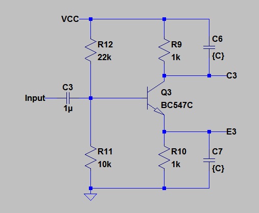
This is the circuit that I used.

You see I used an npn transistor, but just about any active device except an SCR or a TRIAC could be used. Old fogies will remember it being used as a phase splitter in valve amplifiers. I don’t know whether it is popular in latter day valve amplifiers as are used in electric guitar service.
I recently saw it in a final year project report that was written by a friend in 1962.
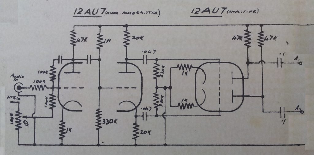
The “Concertina” is the second triode. Note the twin triode to the right acting as a buffer on the concertina stage outputs. Maybe this is significant. See below. Note that in those days, circuits were simpler, and the argument that one might make these days that it is important to show active devices the right way up for clarity (an argument that I hold to), had not really come into effect.
My title for this post included the words “A gift that keeps on giving”. The reason for this is that there are two extra aspects of complexity that never arose when I was using this circuit for job interviewing. In all its simplicity, it is really more complex than I realized.
Gift 1.
I had actually been aware of this years before I ever conducted a job interview, but I hadn’t thought of it in the context. The argument goes that one possible problem with the circuit is that the two outputs have different impedances, so that they will suffer to different extents if capacitively loaded. For discussion of this, I will stick to the npn transistor case, but the argument holds for the 12AU7 as well. The output on the collector will have an impedance which will be the parallel connection of the 1k load resistor and the resistance of the collector itself. For practical purposes we can take this to be the load resistor alone. That is 1k.
The output impedance at the emitter on the other hand will be the load resistor in parallel with Re
Re = 25E-3/Ic
= (approx) 25E-3/3.15E-3
= 8 ohms
In this case, it is the load resistor that becomes insignificant, and we can say that the output impedance at the emitter is eight ohms.
Let us imagine that we load each output with a 100nF capacitor. We might expect that the Collector output will droop at high frequencies with a pole constructed of the 1k output impedance and the capacitor.
RC = 1E3 * 100E-9
= 100 us
Break freq. = 1.59 kHz
Similarly, at the emitter, R = 8 ohms
RC = 8 * 100E-9
= 800 ns
Break freq. = 199 kHz
This is not how it works out, however. The capacitor on the emitter provides emitter bypassing, so that as the frequency at which the capacitor breaks with the emitter load resistor is passed, the gain of the transistor as a common emitter stage starts to rise. Over the next decade, this rise cancels exactly the fall in output at the collector due to the shunting by the capacitor there.
Here are three cases:
Case 1. 100nF Capacitor on Collector.
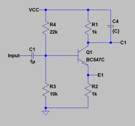
Here are the Bode plots for the outputs.
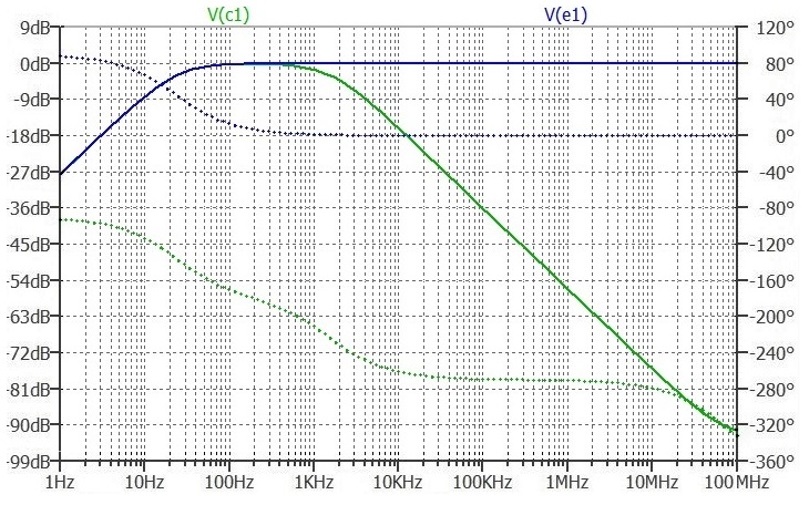
At the low frequency end, the gain is limited by the coupling capacitor on the input.
The Green line represents the Collector. The pole at 1.59 kHz is evident.
The Blue line represents the Emitter. No high frequency attenuation in the frequency range of interest.
Case 2. 100nF Capacitor on Emitter
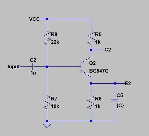
Here are the Bode plots for the outputs.
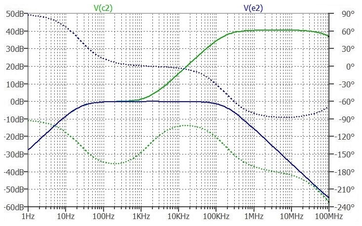
The Blue line represents the Emitter. Notice that the bandwidth at the Emitter is limited by the pole at 199 kHz as predicted in the above sums.
The Green line shows the voltage at the Collector. Note the zero at 1.59 kHz which takes effect as the capacitance on the Emitter breaks with the 1k Emitter load resistor.
Above 1.59kHz, the gain rises as Xc on the emitter falls with increasing frequency. This continues up to 199kHz where Xc has fallen to the same magnitude as Re. Above that, Re dominates and the gain flattens out.
Case 3. 100nF Capacitor on Collector and Emitter
Here is the bode plot for the two outputs:
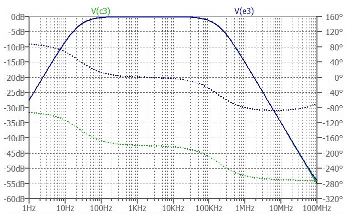
The simulator has drawn the Collector response (Green) first. Then the Emitter response in Blue. The Emitter response overwrites the Collector response for the whole plot, except for up near 100 MHz where the Green line peeps out from under the blue.
The Emitter response (Blue) is the same as in Case 2.
For the Collector response, the pole that was evident in Case 1. is exactly cancelled by the zero that we saw in Case 2.
This result which is, at first blush unexpected, provides a rewarding little bit of sparkle to this circuit. I have to admit that I did not initially think this out for myself. I read an explanation similar to the above in the Wireless World magazine in the 1970s. I found that it fell to me to explain it to a friend recently, so having thought out the explanation properly, I share it with you here. My friend, by the way, suffered from no disadvantage with respect to me except that he is not old enough to have read Wireless World in the 1970s.
Gift 2.
Here is another gem that emerges from the apparent simplicity of this circuit. Unlike Gift 1. I have thought this all out for myself.
One possible application for a phase splitter is to provide a “balanced” output for a connection between items of equipment where there might be some common mode signal between the different local grounds. A “balanced” signal path might be used even where the two grounds are solid, but where magnetically induced or capacitatively coupled interference might advantageously be cancelled.
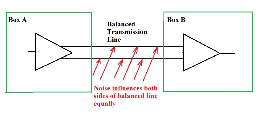
The concertina circuit is NOT suitable for use as the phase splitter to provide the balanced signal in such an application. I have seen it so used (many years ago), but at that time, I didn’t realize what the problem was.
There are two distinct factors at play here. First the two outputs have different output impedances. Any common mode current to both outputs will give rise to a much higher noise voltage on the Collector where the output impedance is about 1k (in our example) than at the Emitter where the output impedance in our example is about 8 ohms.
Earlier in this post, I made a snide remark about drawing active devices lying on their side. One problem with this is that some circuit configuration might inadvertantly arise, and not be immediately recognized as it does not show the active device in the way we are used to. My habit is to strictly constrain the way I draw these things. Although it is common to draw a transistor lying on its front with its nose in the mud when wired in the common base configuration, it need not be. I drew it the right way up when I designed a common base circuit in an earlier Blog post.
Post number 29 “I did the test question – and failed!” 23-07-2014
http://richardschurmann.com.au/Other/Electronic_Burrow/?p=308
This was how I drew my common base circuit on that occasion:
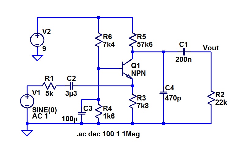
The similarity to our concertina circuit is immediately apparent. To apply a noise current to the Emitter, is to apply it to the input to a common base stage. Whatever current we feed into the Emitter will come out the Collector (ignore base current a.c. component). If the current is a “common mode” current, applies to both outputs, then the Collector will get a double dose. One from the noise source, and one from the collector itself. All this is clearly seen in simulation.
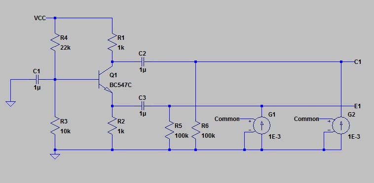
I used a sinusoid of amplitude 1 millivolt and frequency of 10 kHz to provide the signal “Common”.
Here is what we get:
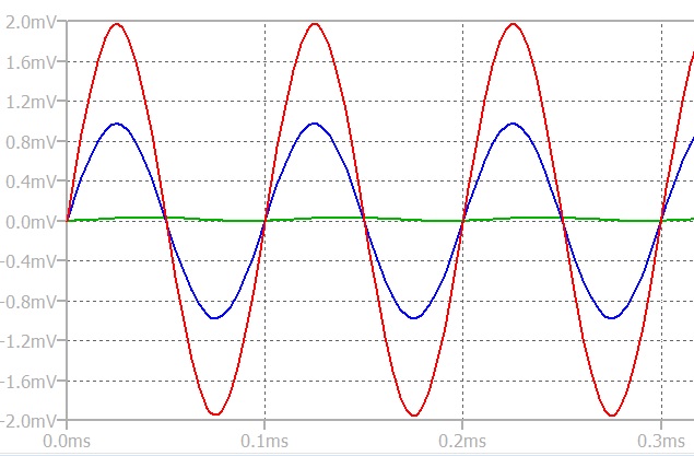
Don’t you worry about absolute magnitudes here. What we are looking at is how the noise voltages on the two outputs compare. The Green trace is the noise voltage on the Emitter.
The Blue trace is the noise voltage on the collector with noise current applied to the emitter only. That is, the signal we see on the collector is there as the transistor is acting as a common base amplifier.
The Red trace is the voltage on the Collector when identical noise currents are applied to both outputs.
I found it interesting that if I placed a 2k resistor in the connection between C3 and the current source G1, then the two outputs have matched noise voltages. This means that if the receiver at the other end of the “balanced” line, has good common mode rejection, then the noise will not appear. This would be a very unsatisfactory circuit though. The balancing of the two noise voltages would be precarious, and anyway, the introduction of the 2k resistor would spoil the matching of frequency responses that I discussed under the heading of “Gift 1.”.
The best way to utilize the Concertina in a circuit with any interference or capacitative loading on the outputs is to isolate it with a buffer stage as shown in the vacuum tube example above. This is almost exactly what Williamson did in his celebrated audio amplifier https://en.wikipedia.org/wiki/Williamson_amplifier design in 1947.
Sorry about those old 12AU7s, Cyril!
In my earlier discussion of the Concertina circuit, I referred the reader to an article on the Concertina circuit at
http://www.r-type.org/articles/art-010p.htm.
Looking at it again now, I am concerned that it might contain piffle. Go into it with care.

